EMS and CEM capacity, SMT and production process, reshoring and plant investment.
The week ending 1 October brought AI deeper into chip design, advanced packaging closer to the centre of semiconductor development and another step towards 800 VDC data centres. Alongside new manufacturing capacity and more capable embedded processors, the common theme was practical: turning ambitious technology into systems that can actually be built.
Gotion will invest €1.1 billion for a 49% interest in PowerCo’s Valencia battery operation. The agreement brings LFP production closer to European vehicle plants while exposing the technical and industrial depth required to localise the complete battery system.
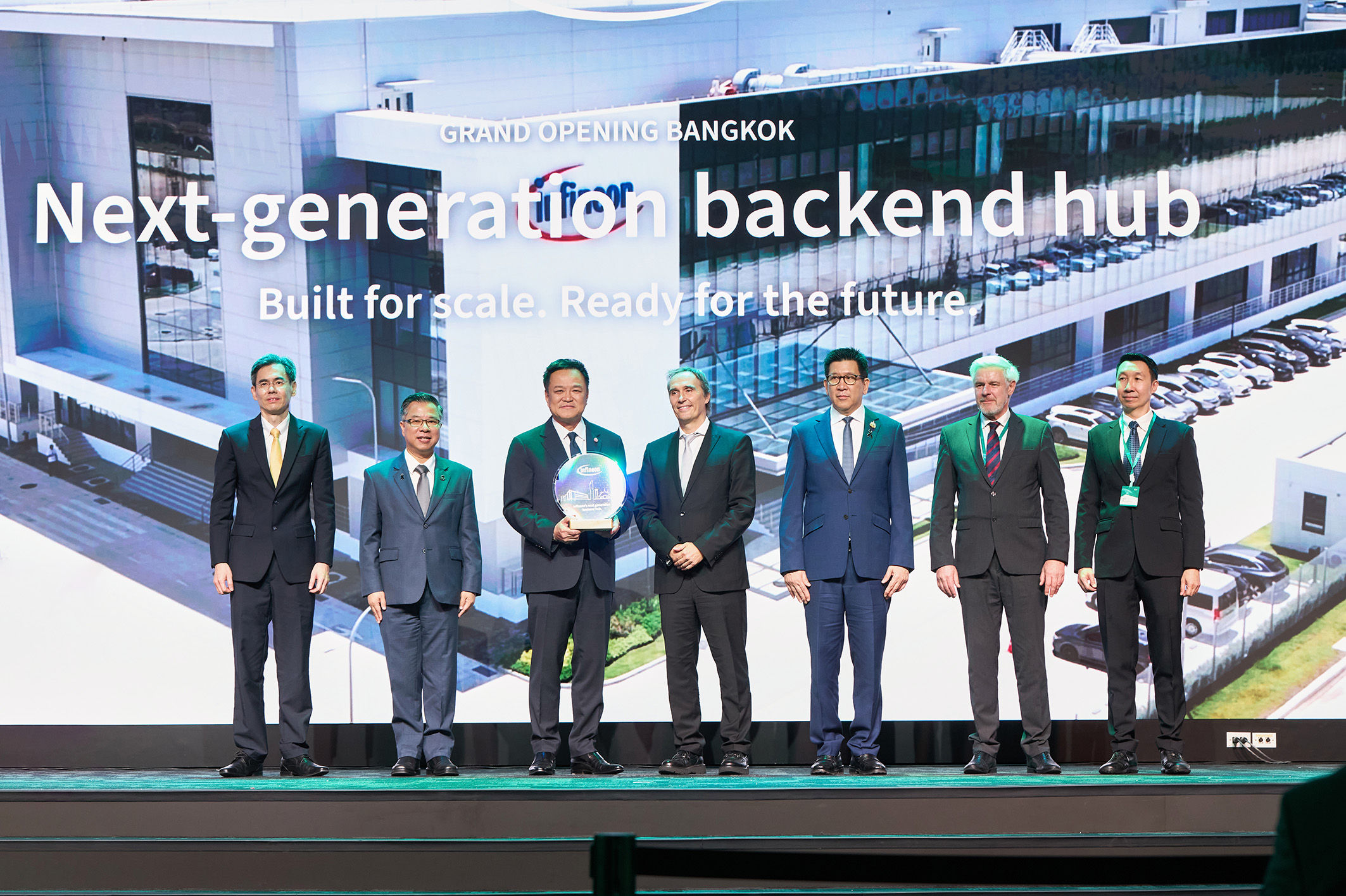
Infineon has inaugurated a greenfield backend manufacturing site near Bangkok, designed to scale to five modules as part of its global capacity diversification.
The US specialist is adding EU data hosting, European distributor links, language support and currency conversion ahead of electronica in November.
The company-supplied system integrates temporary bonding, debonding and detaping, with ERS reporting throughput of 13 panels an hour and a first customer delivery.
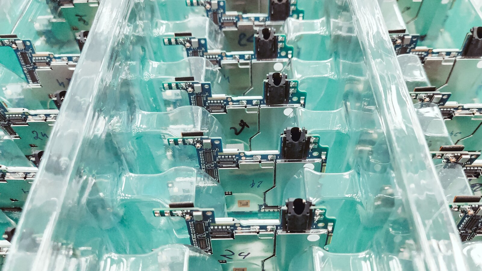
A prototype proves that one build can work. Production must prove that the design still works across component tolerances, process variation, environmental limits and repeated assembly.
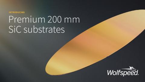
The orderable substrate has a published micropipe limit below 0.01 per square centimetre as device makers assess yield and supply at 200 mm.
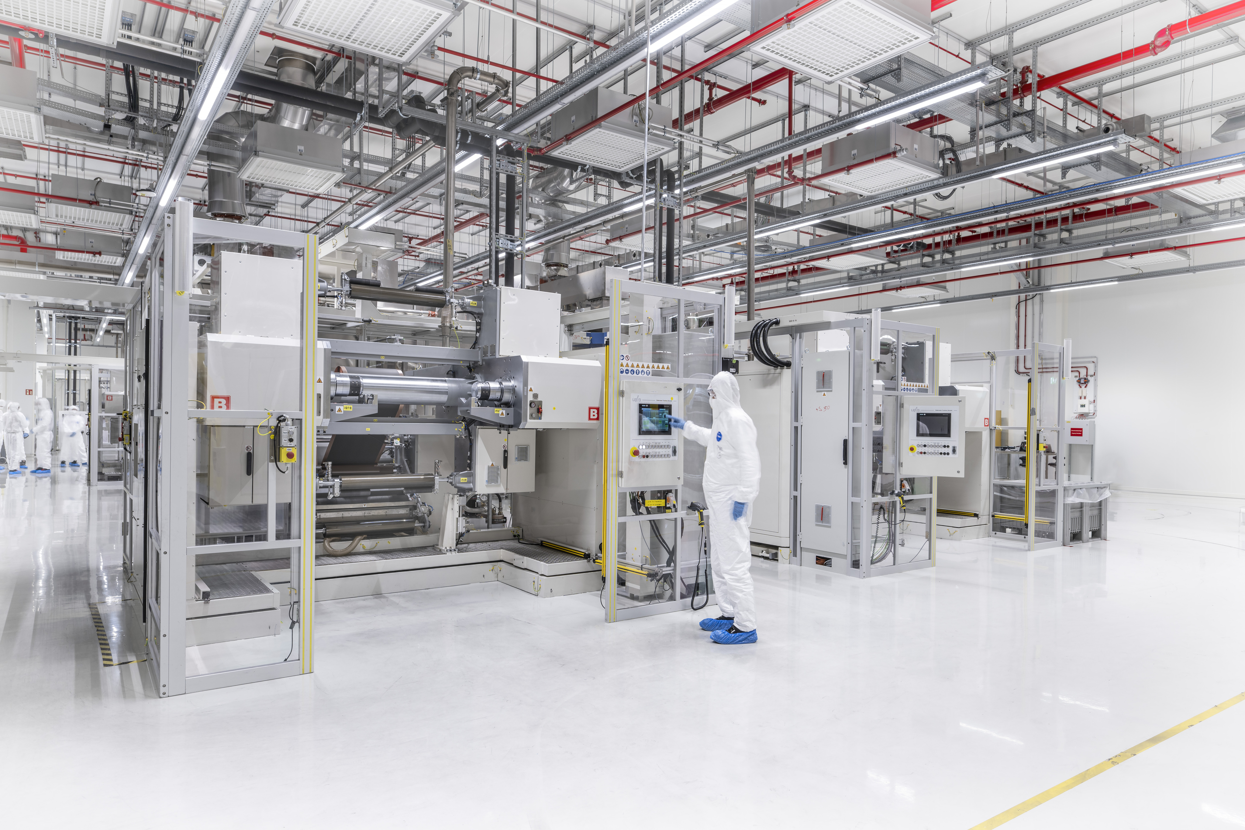
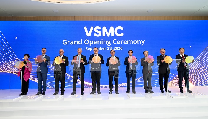
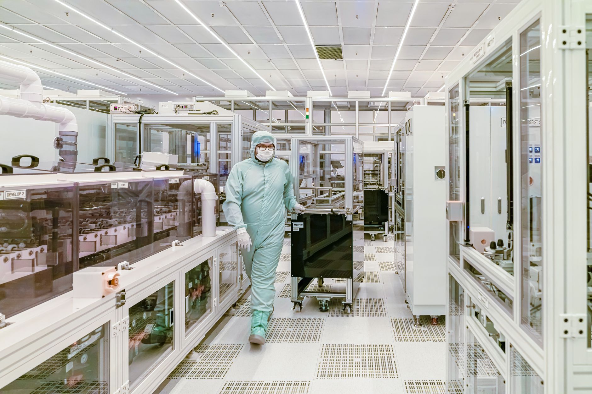
NXP and VIS joint venture VSMC has completed its first 12-inch specialty fab in Tampines, targeting volume production in Q1 2027.
A clean design rule check is not the same as a production ready data package. These ten checks can expose the mismatches, omissions and assumptions that delay fabrication or produce the wrong board.
The licensable I/O IP lets advanced-node chips connect to higher-voltage parts, with integrated ESD protection and a regulator for the 3.3 V N4C implementation.
EU ministers back stronger semiconductor capacity, simpler rules and investment across the value chain. For electronics businesses, Chips Act 2.0 will be judged by delivery.
GSME and Teradyne have announced a partnership to establish a semiconductor test and evaluation centre at GSME’s new Silicon Valley headquarters.
The collaboration covers certified A14 flows, CoWoS multi-die support and co-packaged optics, while the claimed productivity gains remain supplier assertions.
The week ending 24 September showed how far demand for AI infrastructure is reaching into the electronics supply chain. Memory, optical links, power components, production equipment and country of origin are all becoming part of the same calculation.
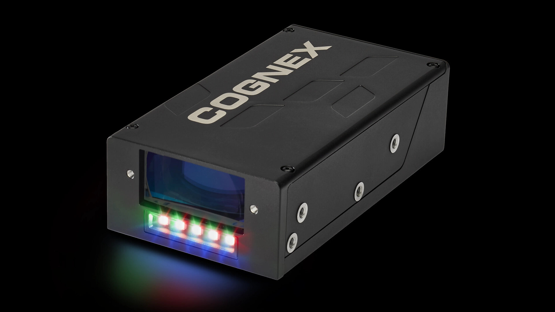
The new wafer and panel identification system targets degraded marks and difficult substrates, but buyers will still need evidence from their own processes.
Component declarations support compliance, but UK manufacturers still need product-level evidence, production controls and a defensible link from the design to the declaration.
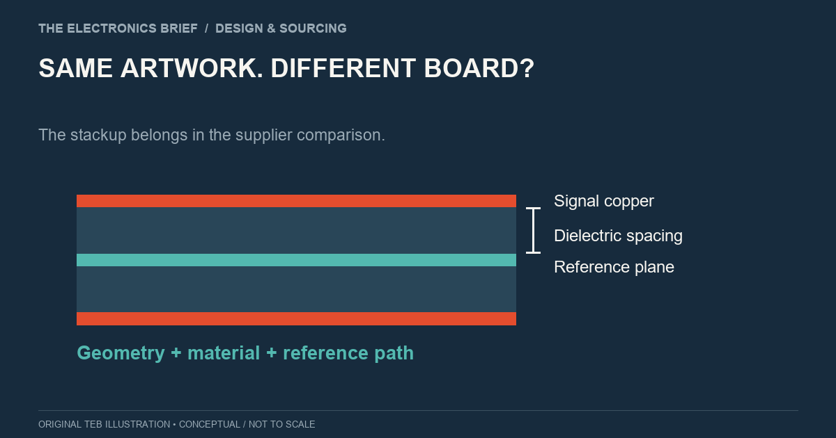
A different fabricator may propose a different stackup, even with the same copper artwork. Check the construction while there is still time to compare the true cost.
Vishay has introduced four surface-mount rectifier series rated 5 A to 12 A in a new 0.88 mm DFN6546A package with wettable flanks, some in AEC-Q101 qualified versions.
Nordic, TDK, ST and imec supplied new device and process detail, while a government study put firmer numbers around the UK semiconductor sector. Here is what design and purchasing teams should verify next.
Imec has shown research-stage NbTiN Josephson junction circuits and 30nm superconducting interconnects aimed at future HPC, AI and quantum computing hardware.
UK electronics output rose in the latest official figures, while developments in wafer materials, connectors, legacy parts, embedded design and data-centre power offered a more complicated picture. Here is what changed during the week ending 11 September — and what design and purchasing teams can usefully check next.
Imec's 30nm NbTiN interconnect demonstration improves the manufacturing case for superconducting computing, but design tools, cryogenic integration and system economics remain as important as device density.
Imec and its material suppliers report single-exposure High NA EUV patterning of 22nm-pitch logic structures using established chemically amplified resist technology.
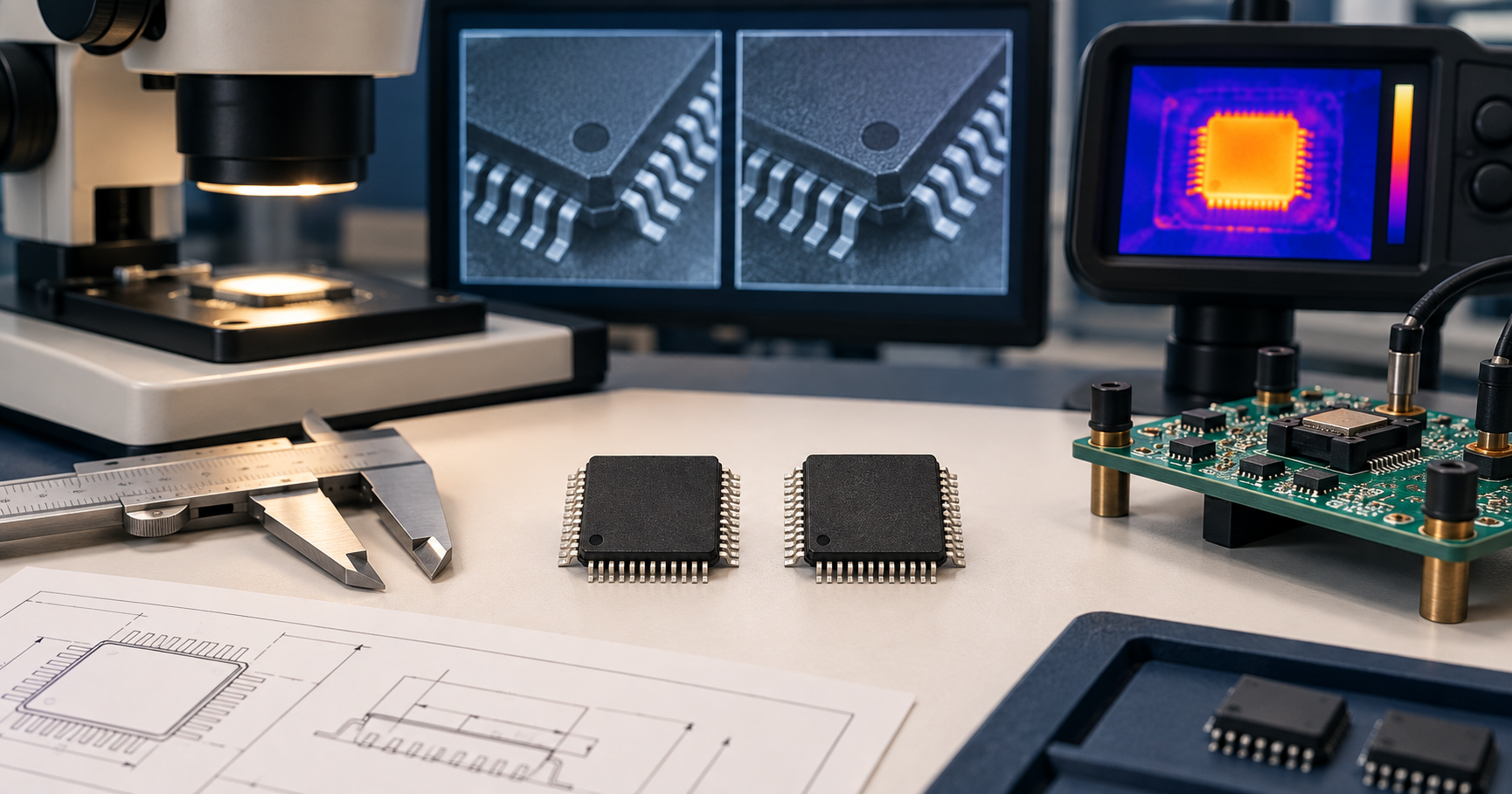
Matching headline specifications is only the start. A disciplined comparison covers construction, limits, behaviour, supply route and the evidence needed to approve the alternative.