Xintec to run advanced packaging line at TSMC’s Taichung site
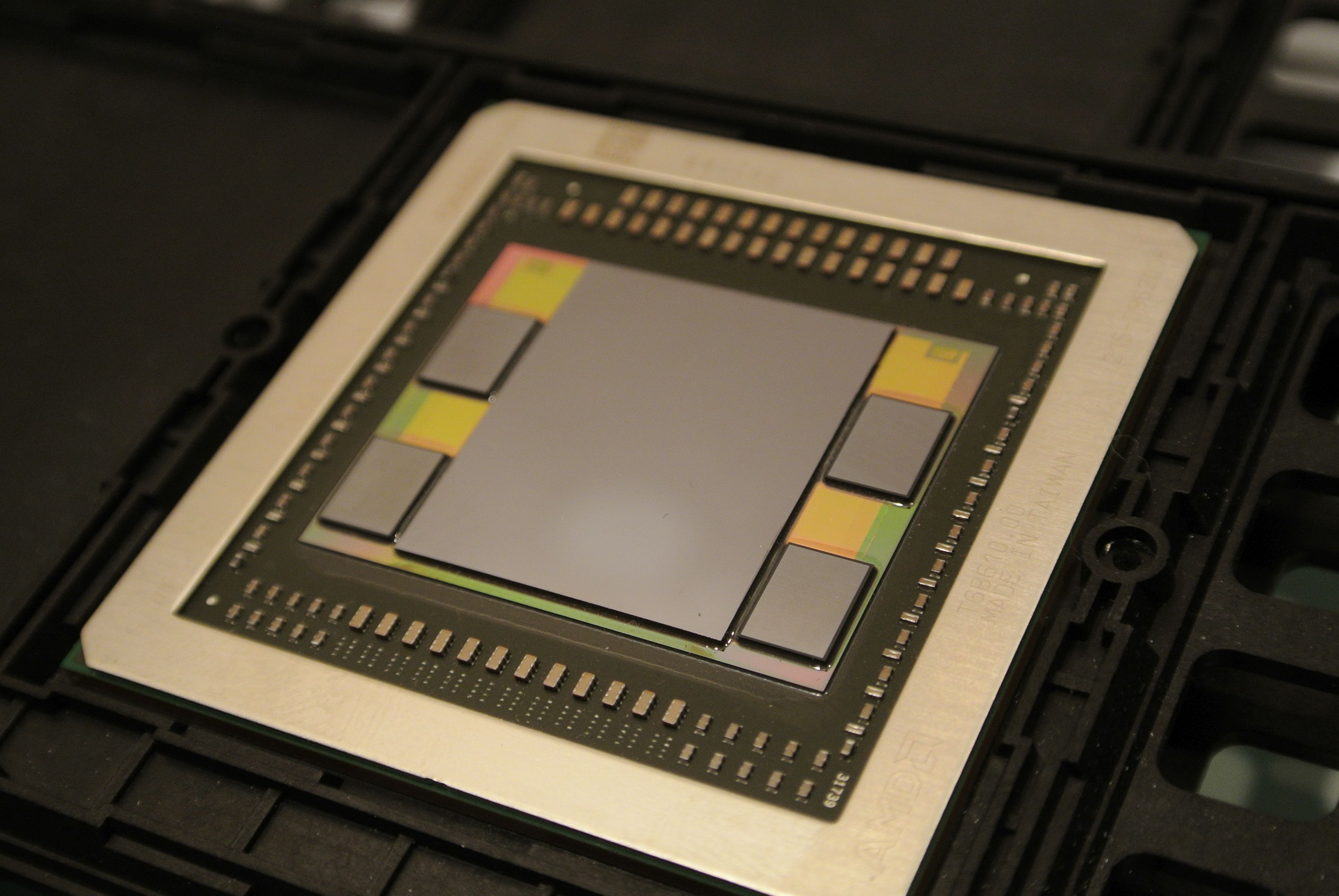
Image: Illustrative AMD Fiji package. C. Spille / pcgameshardware.de via Wikimedia Commons · CC BY-SA 4.0
Xintec will buy the production and automated handling equipment for an advanced packaging line inside TSMC’s Central Taiwan Science Park facility, then run it under an outsourcing agreement that lasts until the end of 2033. The first phase is due to reach volume production in 2029 and will handle what the filing calls the on-substrate stage: mounting an already assembled set of chips onto the package substrate.
By the time an assembly reaches that stage in a typical chip-on-wafer-on-substrate package, the processor and high-bandwidth memory are already connected through an interposer. The substrate underneath serves a different purpose: it carries connections from the assembled device out to the circuit board and distributes power back into the package. Putting more equipment on this step gives TSMC another way to handle assemblies ready for mounting, though finished output will still depend on how many processors, memory stacks and interposers make it through the steps before it.
The arrangement shares responsibility for how the line performs. Xintec will equip and run it, drawing on TSMC’s packaging technology and manufacturing support to meet the process, quality and yield requirements. Xintec’s board approved NT$15 billion in convertible bonds to fund that initial capacity, but the filing gives no throughput figure and leaves the package variants and end customers unnamed.
Sources: Xintec’s exchange disclosure, reproduced by MoneyDJ; TSMC’s description of its chip-on-wafer-on-substrate packaging.