Infineon processes first 300mm power SiC wafer
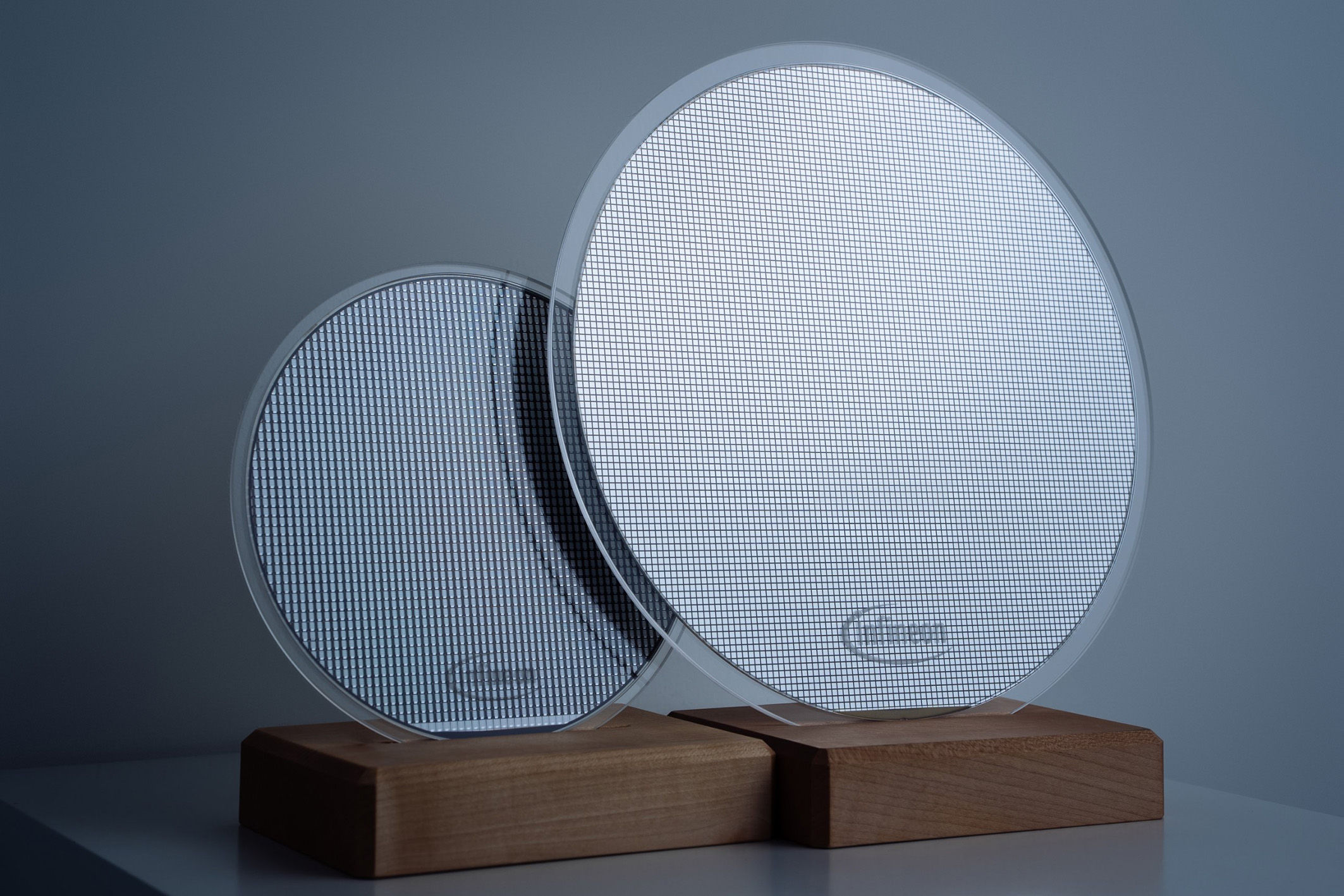
Image: Infineon
Infineon has produced functional power devices on 300-millimetre silicon carbide wafers at its Villach, Austria fab, a step it describes as the first time this has been achieved in a full-scale semiconductor manufacturing environment. The company says the work was carried out using existing silicon production equipment rather than a dedicated new line.
Infineon states that a 300 mm SiC wafer yields 2.3 times more chips than a 200 mm wafer, reflecting the larger surface area available per wafer. This figure is Infineon's own comparison and relates to die count per wafer rather than cost or yield outcomes.
The achievement is described as a feasibility milestone rather than a production changeover. Infineon says it will plan 300 mm SiC technology and ramp timing in consultation with customers and partners while continuing to execute its existing 200 mm SiC manufacturing roadmap, indicating that 200 mm remains the current supply basis.
Cold Split process also proven at larger diameter
Separately, Infineon says it has proofed the feasibility of its Cold Split wafer-separation technology on 300 mm SiC at its Dresden site. Cold Split separates wafers from a SiC boule, which Infineon states involves less material loss and substantially reduced processing time compared with conventional wire sawing, allowing more wafers to be obtained from the same crystal at lower capital expenditure. As with the 300 mm device result, this is presented as a feasibility demonstration rather than a qualified production process.
Infineon positions SiC as material for power conversion in traction inverters, on-board chargers, EV chargers, large-scale energy storage, industrial drives and uninterruptible power supplies, and cites emerging use in AI data centre applications including solid-state transformers, circuit breakers and power supply units. These application statements are Infineon's own characterisation of demand.
The 300 mm SiC work follows Infineon's announcement on 27 October 2026 of an approximately €1.1 billion investment in a high-volume manufacturing facility for GaN power semiconductors on 300 mm wafers, also in Villach. Infineon says it now has processed capability across silicon, silicon carbide and gallium nitride at the 300 mm diameter, though for GaN this relates to the separately announced manufacturing investment rather than the SiC feasibility result reported here.
Infineon plans to display the first processed 300 mm SiC wafer at the electronica trade show in Munich, running 10 to 13 November 2026, in Hall C3, Booth 502.