Why is a DC-DC converter overheating? Losses, PCB layout and cooling
A DC-DC converter can run hot well below its headline current rating because the rating does not describe every combination of input voltage, switching conditions, PCB construction and enclosure temperature. The same device may behave comfortably on an evaluation board and struggle in a compact assembly with less copper and warmer surroundings.
There are two connected questions behind the temperature: how much power is becoming heat and how effectively that heat leaves the components. Separating them helps explain why a larger regulator or an added heatsink can produce less improvement than expected. Either change may be useful, but its value depends on the cause of the temperature rise.
Efficiency puts a number on the conversion loss
Input and output voltage measured at defined points on the assembly, together with the corresponding currents, establish the conversion boundary. Wiring losses and instrument burden can distort the result, particularly at light load where a small current measurement error has a larger relative effect. Nisshinbo’s guidance discusses these measurement limitations. [1]
For a steady operating point:
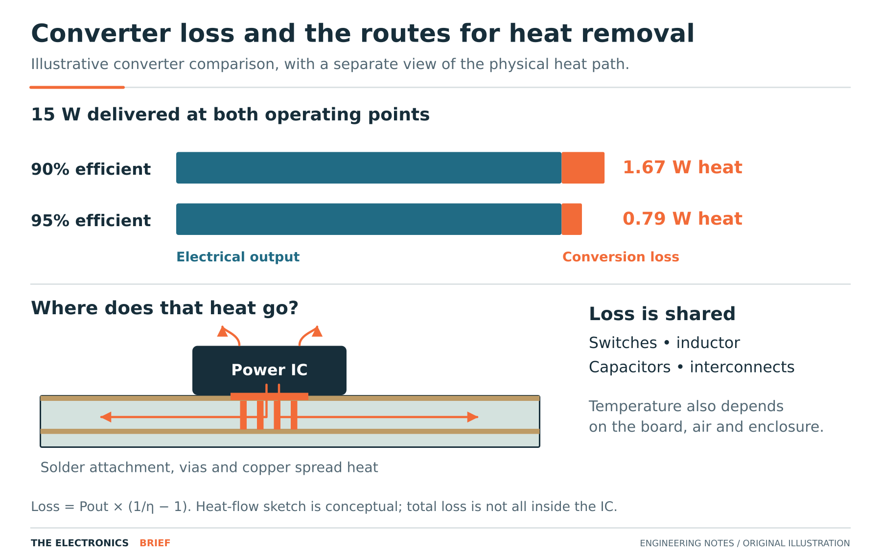
Ploss = Pout × (1/η − 1)
At an illustrative 5 V and 3 A, the converter delivers 15 W. Efficiency of 90% implies approximately 1.67 W of loss, compared with 0.79 W at 95%. Those five percentage points more than halve the power that has to leave the assembly as heat.
The loss belongs to everything inside the measurement boundary. Switches, inductor, capacitors and interconnects can share it, so assigning the entire figure to the regulator IC would overstate its dissipation. Where voltage and current vary significantly over time, an appropriate average power measurement is needed because multiplying separately averaged values can give a different result.
The comparison becomes more informative across the intended input voltage and load range, where the balance of losses can change.
Different loss mechanisms leave different clues
In a synchronous buck converter, switch conduction and transition losses, gate drive consumption and the inductor’s copper and core losses contribute in different proportions. A rise dominated by current squared suggests a different investigation from one that follows switching frequency, with the manufacturer’s model or loss guidance helping to interpret the result.
Capturing switching loss directly introduces its own measurement demands. Tektronix explains why voltage and current probes need correct timing alignment: a small delay between the traces can create a substantial error when instantaneous power is integrated across fast transitions. [2]
The inductor’s two current ratings describe different limits. Saturation current relates to a specified reduction in inductance, while a thermal current rating relates to an allowed temperature rise under stated test conditions. Coilcraft discusses the distinction and the effect of the application environment. [3]
An inductor may retain adequate inductance at peak current yet dissipate too much power in the enclosure. Conversely, a significant inductance reduction can alter the waveform and increase stress elsewhere. Ripple and peak current therefore help explain behaviour that the average output current alone leaves unresolved. In an asynchronous converter, the rectifier’s forward drop and conduction interval add another loss contribution.
The PCB is part of the thermal path
An exposed pad can provide a substantial route from the package into the board, depending on its solder attachment, land pattern, thermal vias and connection to spreading copper. Layer count and copper area also affect how far the heat can spread before reaching the surrounding air or enclosure.
This is one reason evaluation board temperatures do not transfer directly to another layout. Two boards with similar component placement can have quite different connections between copper layers, while neighbouring components change the local thermal conditions.
TI’s thermal metrics note states that “RθJA is not a constant”. Thermal resistance from junction to ambient depends on the board and environment used for the measurement, so a datasheet value needs that context before it is used to estimate a temperature in another assembly. [4]
A measured package top temperature also requires interpretation. Where the manufacturer supplies an appropriate ΨJT characterisation parameter, it can support an estimate of junction temperature using that device’s dissipation. It is not interchangeable with thermal resistance from junction to case, and the dissipation estimate must exclude losses belonging to other components. [4]
The enclosure changes the operating conditions
Local air temperature and the time allowed to approach thermal equilibrium affect the comparison between bench and enclosed operation. The enclosure may restrict airflow, provide a useful conduction path or place the converter beside another heat source, so the finished arrangement belongs in the measurement.
Infrared readings depend on emissivity, reflections and access, while a thermocouple can also disturb the point being measured. Consistent measurement positions and methods help relate the temperature distribution to electrical losses and make a later board revision comparable.
Controlled airflow can help distinguish heat removal from loss generation. If temperature falls while measured input and output power remain essentially unchanged, the experiment supports an improvement in the thermal path at that operating point.
A corrective change follows from the measured cause
Higher switching loss may justify a power stage change, while excessive inductor dissipation may call for a part better suited to the waveform. A restricted thermal route may instead respond to changes in solder attachment, spreading copper or the connection to the enclosure. A heatsink has a role where there is a useful path into it and a way for it to shed the heat.
The resulting engineering change can describe the specific layer, node or component involved and the measurement that supports it. Retesting the original worst operating conditions, startup and transients then establishes whether the cooler assembly still meets the converter’s electrical requirements throughout its intended range.