Why an ion trap and its optics might be made on different wafers
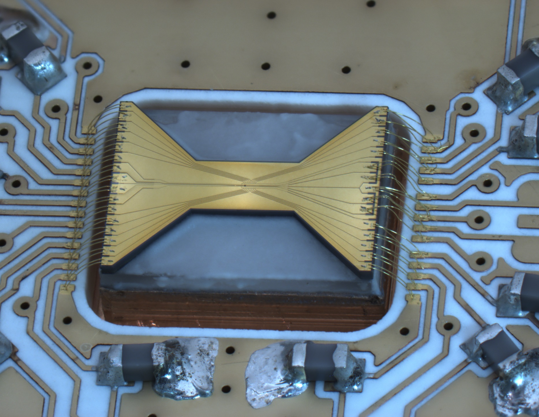
The electrodes in a surface ion trap create the fields that hold ions above the chip. An optical circuit has a different job: it can carry light through waveguides and direct it towards the ions with structures fabricated on the chip. Making those parts separately gives each process more freedom over its materials, but the optical circuit still has to line up with the points where the trap holds its ions.
EV Group says it worked with researchers on a low-temperature metal bond to join trap and photonic chiplets made on dissimilar substrates. Bonding at a lower temperature can help limit relative movement as the two materials cool if they expand and contract at different rates. It also reduces the amount of heat the already fabricated structures have to tolerate. EVG’s 9 November release did not identify the materials or give a bond temperature, alignment tolerance or post-assembly optical loss for this work.
An independent experiment published in Light: Science & Applications gives some context for why the alignment matters. The researchers brought their waveguide outputs to a spacing of 8 µm and used a trapped ion to measure light spilling from other channels. They reported intensity crosstalk below roughly one part in a thousand across the chip. That is the kind of result a bond inspection alone cannot give. The work was a separate demonstration, not a performance result for EVG or CHAMP-ION.
CHAMP-ION, led by Silicon Austria Labs, plans to make process design kits available for standard and customised ion traps. Its published plan includes fabrication, packaging and testing services, with initial access scheduled for early 2028. The consortium describes photonic integration as a technology it intends to evaluate for future offerings; it has not listed EVG’s research bond as an orderable process.
Sources: EV Group’s process announcement; CHAMP-ION technology and timetable; Research on integrated optical addressing of trapped ions.