Weekly briefing: Electronics starts to rethink how it builds

AI-generated editorial illustration for The Electronics Brief. Conceptual artwork, not a depiction of the actual glove.
Building a better chip is no longer just a question of what goes inside it.
This week’s announcements reached into the tools engineers use, the connections between semiconductor dies, the electricity feeding server racks and the factories preparing devices for shipment.
The most eye-catching development was a partnership intended to make AI a specialist user of chip-design software. But some of the equally consequential changes were physical: new approaches to packaging, power conversion and manufacturing.
Taken together, they suggest an industry reconsidering the whole route from an engineering objective to a working product.
AI moves from helping engineers to operating their tools
On 30 September, Synopsys and OpenAI announced a multi-year partnership to develop GPT-Synopsys, a specialised model intended to operate electronic design automation tools.
The ambition goes beyond answering technical questions or suggesting code. The companies describe a system that would run design tools, interpret results, change a design and repeat the process towards objectives set by engineers. Early technology engagements with semiconductor customers are underway.
That is a potentially important change in how engineering work is divided.
If successful, it could let teams explore more alternatives before committing to a design, with engineers spending more time setting constraints and reviewing results.
The qualification matters. This is a development partnership, not proof that autonomous chip design has been solved. The announcement does not establish independently measured improvements in development time or successful silicon.
The interesting question is no longer whether AI can produce plausible engineering output. It is whether it can consistently produce verifiable results inside the tools on which manufacturing decisions depend.
Advanced packaging becomes part of the architecture
Applied Materials and Besi expanded their partnership on 1 October, with Besi joining Applied’s EPIC Center as an Innovation Partner.
Their work will extend beyond existing die-to-wafer hybrid bonding into additional bonding platforms and architectures, including die-on-die and die-on-panel approaches. The stated targets include closer integration of logic, memory and photonics for AI infrastructure.
The significance is not simply that two equipment suppliers are collaborating more closely. It is that packaging is increasingly part of the computing architecture, rather than something decided after the silicon.
Bringing different functions together creates opportunities to improve a system without relying entirely on a smaller transistor process. It also makes the interfaces between those functions more consequential.
Our reading is that this strengthens the case for involving packaging and manufacturing expertise earlier in development. A promising architecture still needs a credible route through assembly, inspection and test.
This week’s announcement sets a direction for that work. It does not mean every proposed integration method is ready for high-volume production.
The AI power problem reaches the grid connection
Infineon and Eaton announced a collaboration on 29 September focused on solid-state transformers for emerging 800 VDC data-centre power architectures.
Infineon will supply silicon carbide devices for Eaton’s medium-voltage solid-state transformer 2.0 platform, intended for deployment across Asia-Pacific. The companies say the platform reduces conversion stages compared with conventional architectures. They are also exploring future systems using 2.3 kV and 3.3 kV SiC modules.
This moves the discussion beyond choosing a more efficient component inside a server power supply. It concerns how electricity reaches the computing equipment in the first place.
The attraction is clear: removing conversion stages could improve the overall power chain. But a new architecture must earn its place through reliability, protection, serviceability and real operating performance, not just a compelling efficiency argument.
For the wider electronics supply chain, the implication is substantial. Power semiconductors are becoming part of infrastructure decisions that shape an entire facility.
The announcement is a concrete supplier collaboration, although it should not be read as evidence that 800 VDC distribution has already become standard across data centres.
Manufacturing expansion is about more than wafer fabs
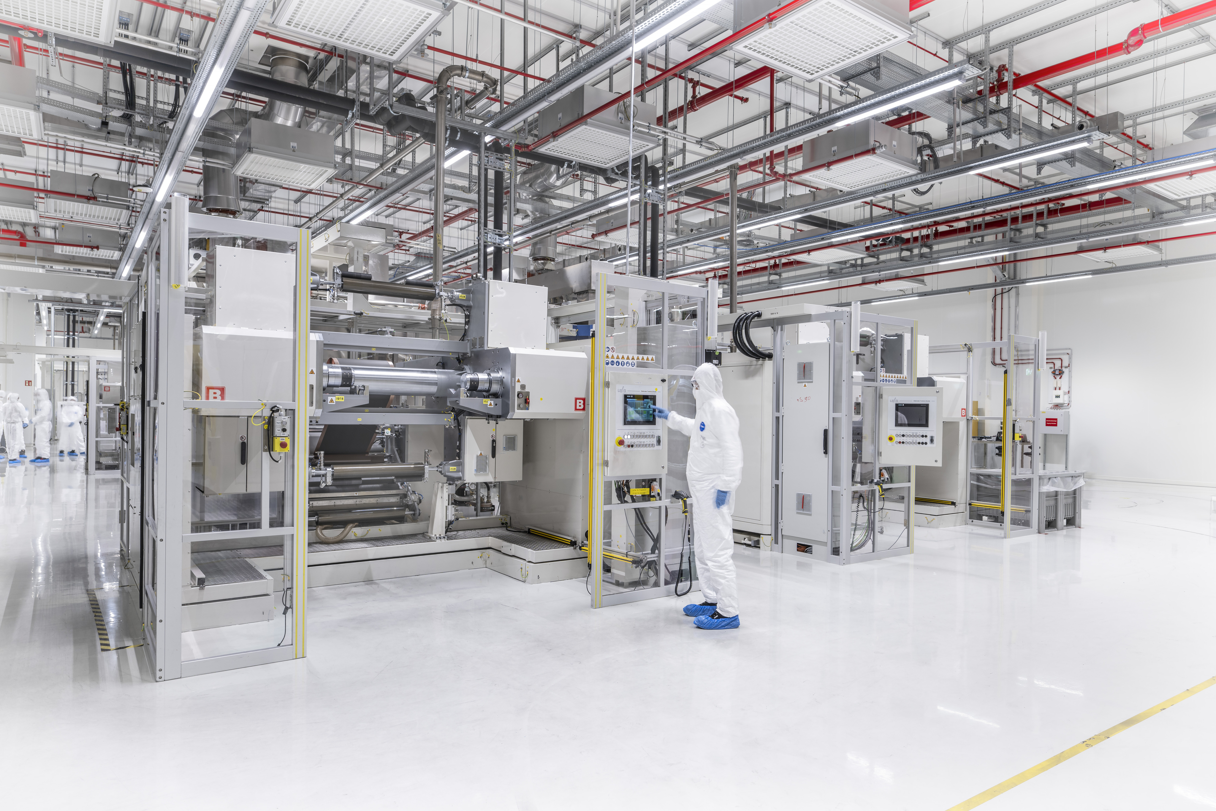
Infineon also opened a new backend manufacturing site in Samut Prakan, near Bangkok, on 1 October.
The facility is designed for phased expansion to as many as five modules. It currently employs around 350 people, with employment expected to reach approximately 1,000 as the first building ramps up. Infineon positions the site as an addition to its geographically diversified manufacturing network.
Backend manufacturing rarely commands the attention given to a new wafer fabrication plant. Yet assembly and test remain essential steps between processed silicon and a component a customer can use.
The commercial significance is therefore broader than another factory opening. Manufacturers need capacity across the production chain, together with the flexibility to support changing product mixes.
For buyers, however, an opening ceremony is not the same as immediately available, fully qualified capacity for every device.
The useful questions concern which products will run there, how production will ramp and when customers can rely on the additional output. The expansion is real; its full contribution will develop over time.
Embedded RISC-V gains more room to grow
Away from hyperscale infrastructure, Efinix introduced its Sapphire RV64 processor core on 28 September, extending its FPGA-based embedded offering into 64-bit RISC-V.
The company is targeting applications that have outgrown the memory, cache and interface limits of its 32-bit cores. Features include an optional memory management unit for Linux support and support for external memory technologies including LPDDR4x.
The important point is not that 64-bit processing is new. It is the additional choice available to designers who want a processor alongside configurable FPGA logic.
That combination can be useful where software must work closely with specialised interfaces or hardware acceleration.
There is a practical caution here too. A wider architecture does not automatically make an application faster or more efficient. Results depend on the workload, configuration, memory system and resources used.
Nevertheless, this is a tangible product development rather than a distant research promise. It gives embedded teams another route to more demanding software without immediately abandoning the configurable platform around it.
The pattern beneath the announcements
Our reading of the week is that the industry is pursuing two changes at once.
One is to automate more of the work required to design complex electronics. The other is to reconsider the physical systems needed to connect, power and manufacture them.
Those ambitions meet at the same difficult point: verification.
An AI-generated design needs checking. A new package needs a viable production process. A power architecture needs dependable operation. Additional manufacturing capacity needs qualification.
The biggest announcements are therefore worth watching not just for their ambition, but for the evidence that follows: measured performance, customer adoption and repeatable production.
That is where an exciting technology becomes an important industrial change.
Something you might have missed? A glove that could help teach robots
The next useful input device for AI might be something you wear on your hand.
Murata announced a partnership with Melt Interface Technologies on 28 September. One of their first joint efforts is the ContactGlove3 Pro, which uses electromagnetic sensing to estimate finger positions and orientation, incorporating Murata’s miniature three-axis LF antenna technology.
The companies envisage applications in robot learning, remote operation and capturing skills used in manufacturing. The glove is due to be exhibited at CEATEC from 13 to 16 October, so that demonstration is still ahead.
It is a refreshingly physical counterpoint to the week’s software announcements.
A skilled person can perform a movement that is awkward to describe in words. Capturing that movement reliably could provide another way to communicate with a machine.
Whether that translates into robust industrial use remains to be demonstrated. But it is a reminder that better AI will need better ways to sense the world, not simply more computing power.
Sometimes, the interface is the interesting part.