I²C sensor standby current: where does power enter when VDD is off?
AI-generated illustration: The Electronics Brief
Fictional case study; measurements and outcomes are illustrative.
Last week’s answer: the first SPI read preceded peripheral readiness
The first SPI exchange took place at 1.5 ms in standalone operation and around 120 ms during a debug launch. That was a useful lead, but the debugger also brought ground, reset and signal connections into the experiment.
Attaching the debugger without starting a session left the cold boot failure unchanged, whereas releasing a controlled standalone reset after the front end’s startup interval restored operation. Measurements at the devices showed acceptable supply and reset conditions in both tests, while the clock and boot configuration were checked against the MCU documentation.
Capturing chip select, clock, data and READY together allowed the team to compare the first read with the front end’s startup specification. The interface was not guaranteed to accept that read until startup had completed, and the standalone transaction arrived too early. The debugger simply took long enough to launch the application that the peripheral was ready by the time it was asked to identify itself.
The firmware was changed to wait for readiness and allow any further delay specified by the device, with a timeout that reported an identifiable fault if startup failed. Initialisation was tested both by cycling the supply and by resetting the MCU while the rest of the board stayed powered. Using the documented readiness condition allowed the sequence to accommodate startup variation, with the timeout providing a response if the peripheral failed to become ready.
The revised unit then passed the defined tests across supply ramps, temperature and reset sequences, including starts with the debugger entirely disconnected.
This week’s challenge: the sensor that will not switch off
A battery powered controller gates the 3.3 V supply to one I²C sensor when it is not needed. The MCU and a second device stay powered, and the shared SDA and SCL lines each have a 4.7 kΩ pullup to the 3.3 V rail that remains on.
The controller should draw about 8 µA in standby, yet with the sensor’s load switch off the measurement is approximately 520 µA. The difference materially affects expected battery life and exceeds what the load switch’s specified leakage can explain under these conditions.
A voltage check finds the gated sensor supply sitting at approximately 1.5 V, with both idle bus lines near 2.1 V. No traffic is being generated, and the MCU pins are configured for open drain operation with their internal pullups disabled. Those are the observations for this case; whether the pin voltages are permitted still needs checking against the selected devices.
Disconnecting the sensor branch from both bus lines brings standby current back close to the expected value. Removing only its 3.3 V supply connection had not done so.
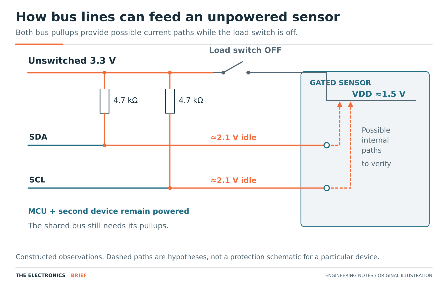
The team suspects a supply path through the signal pins, although it still needs to check the permitted pin voltages and injection current conditions with VDD absent, and inspect the assembly for a bridge or leakage path.
How much current can the bus connections explain?
What current does each 4.7 kΩ pullup deliver with 3.3 V at one end and 2.1 V at the other? Is the combined result consistent with the excess supply current?
Which measurement would distinguish back powering through the signal pins from leakage through the load switch? The second device still needs the shared bus, so any eventual change has to preserve its operation.
TI’s guidance on protection when power is off describes how an input above an unpowered device’s supply can forward bias an internal protection path. Actual behaviour and limits depend on the selected device; an I²C label does not guarantee isolation with the supply off. [1]
The answer follows on 19 November. Share your approach through the Troubleshooter page.