Synopsys and TSMC extend design flows from A14 to multi-die systems
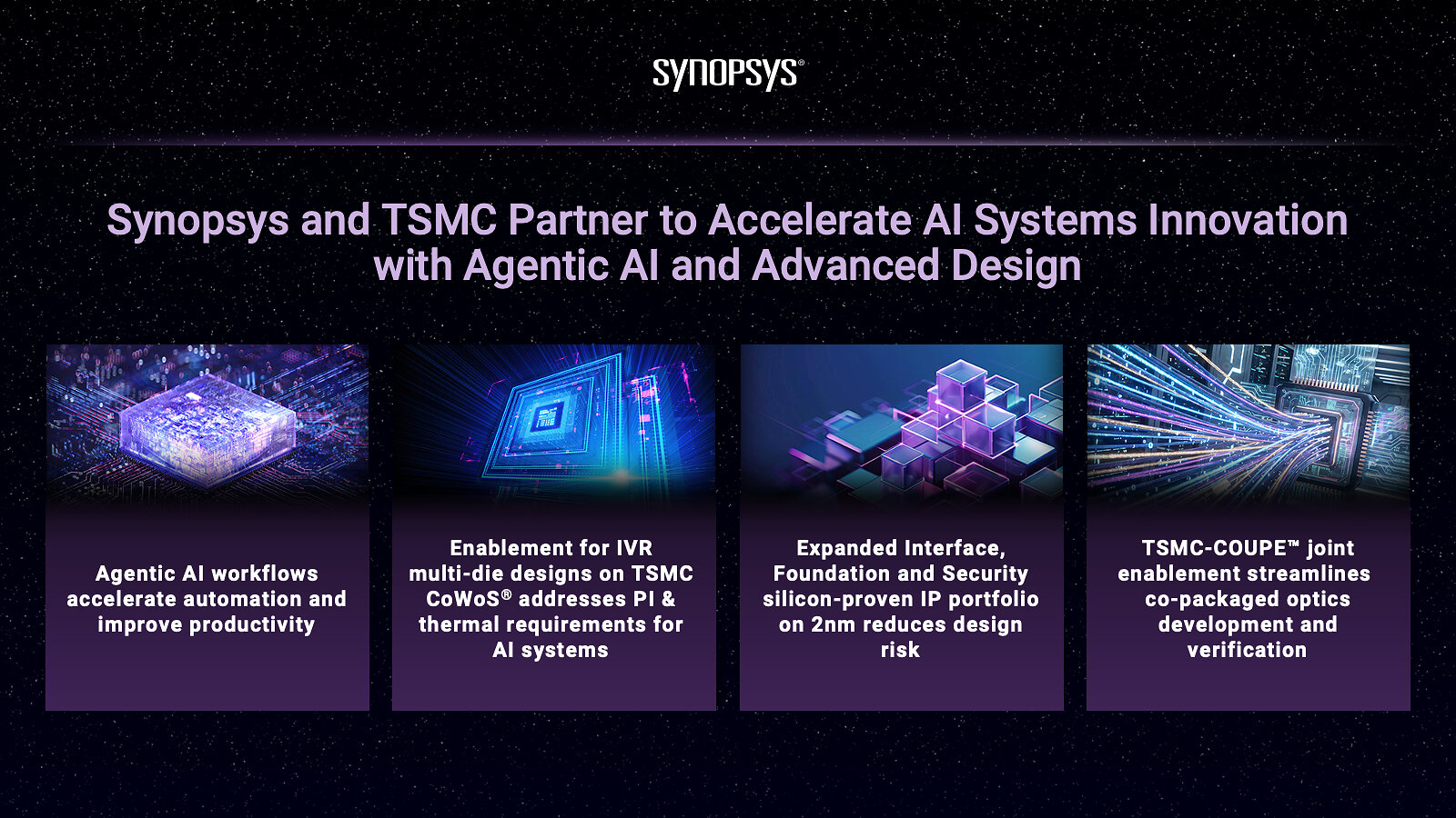
Image: Synopsys
Synopsys has expanded its work with TSMC across A14 design enablement, multi-die packaging and co-packaged optics.
The announcement includes certified digital and analogue design flows for TSMC’s A14 process. Synopsys says the methodology spans implementation through sign-off, with additional work on analogue device routing and AI-assisted engineering workflows.
The scope reaches beyond a single die
The companies are also continuing support for designs using TSMC’s CoWoS advanced-packaging technology. Synopsys says its multi-die flow brings together power integrity, thermal analysis and sign-off tasks for systems in which several dies must operate inside one package.
That package-level view matters because a design can meet an individual die target while still facing power-delivery, heat or interconnect constraints after integration. The collaboration also covers TSMC-COUPE, the foundry’s co-packaged-optics platform, where electronic and optical design decisions must be considered together.
Synopsys has separately highlighted additions to its 2 nm interface and foundation IP portfolio, including PCIe 7.0 and HBM4-related milestones. These should not be confused with the A14 flow certification or treated as one common manufacturing milestone.
A certified flow indicates that tools and methodologies have been assessed for the named process. It does not show that a particular customer device has taped out, reached volume production or achieved a stated performance. Teams assessing the flow should ask which tool versions and design rules are covered, what package configurations have been validated and how the multiphysics sign-off correlates with measured hardware.
Synopsys also describes productivity benefits from agentic AI workflows. The announcement does not provide comparable project data, so those gains remain company claims rather than a demonstrated result across customer designs.