How Qualcomm’s HBC reduces memory transfers during inference
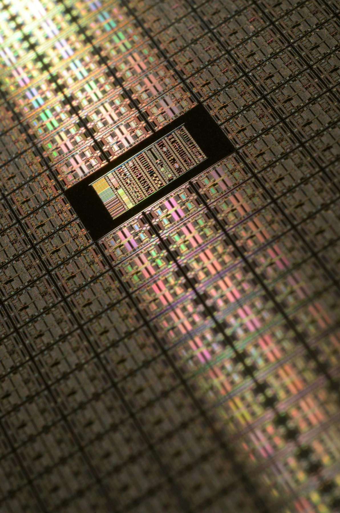
Illustrative image: Laura Ockel on Unsplash
Qualcomm has validated the complete memory read and write path on its first High Bandwidth Compute silicon, running near memory calculations with randomised weights and activations. Automated equipment exercised data paths at production representative dimensions, supporting the technology’s planned use in the Dragonfly AI250 accelerator.[1]
Qualcomm quotes 133 TB/s of effective memory bandwidth and 768 GB capacity for an AI250 card, with the bandwidth figure incorporating computation performed close to the memory. When an operation completes there, its data avoids an external transfer to the main accelerator. The effective figure expresses that architectural benefit, rather than the rate at which bytes physically cross a memory bus.[2]
During language model decoding, model weights and cached attention data must repeatedly feed the arithmetic units. HBC moves selected calculations towards stacked DRAM, reducing some of that traffic and the energy spent moving it. The gain depends on how much work can stay local, since operations that return frequently to the main processor continue to incur transfer costs.
Model structure, precision and cache behaviour therefore affect how well an application uses the architecture. A workload that maps closely to the local compute blocks could obtain a substantial benefit, while another may leave more of that capability unused. Comparing physical memory bandwidth alone would omit the saved transfers, but applying the effective figure to every workload would also misrepresent the result.
Qualcomm bases its comparisons on measured first generation silicon normalised to target operating conditions, using published competing specifications. It qualifies the estimates by implementation, workload and system configuration. The AI250 figures are consequently supported by hardware measurements but remain estimates for the intended product, rather than results from a shipping card.[1][2]
To manufacture HBC, Qualcomm has developed wafer bonding across several process generations and incorporated redundancy, remapping and tests for defects in memory and interface paths. A data centre product has taped out and a logic base with bonded DRAM tiers is being brought up.[1]
Detecting a defective region before bonding, or remapping around it afterwards, can prevent the loss of an otherwise usable stack. The assembly must then maintain bond integrity and acceptable thermal behaviour with logic and memory operating together. Qualcomm says its programme tests those failure modes, though production yield figures have not been published.[1]
AI250 is expected to sample in the first half of 2027. Application throughput and card power measurements will allow its memory capacity, local computation and external transfers to be assessed together, using a stated model, precision and latency target.[1]
Sources
- Qualcomm, HBC silicon validation and manufacturing path, 2 November 2026
- Qualcomm, Dragonfly AI250 product targets and qualification notes
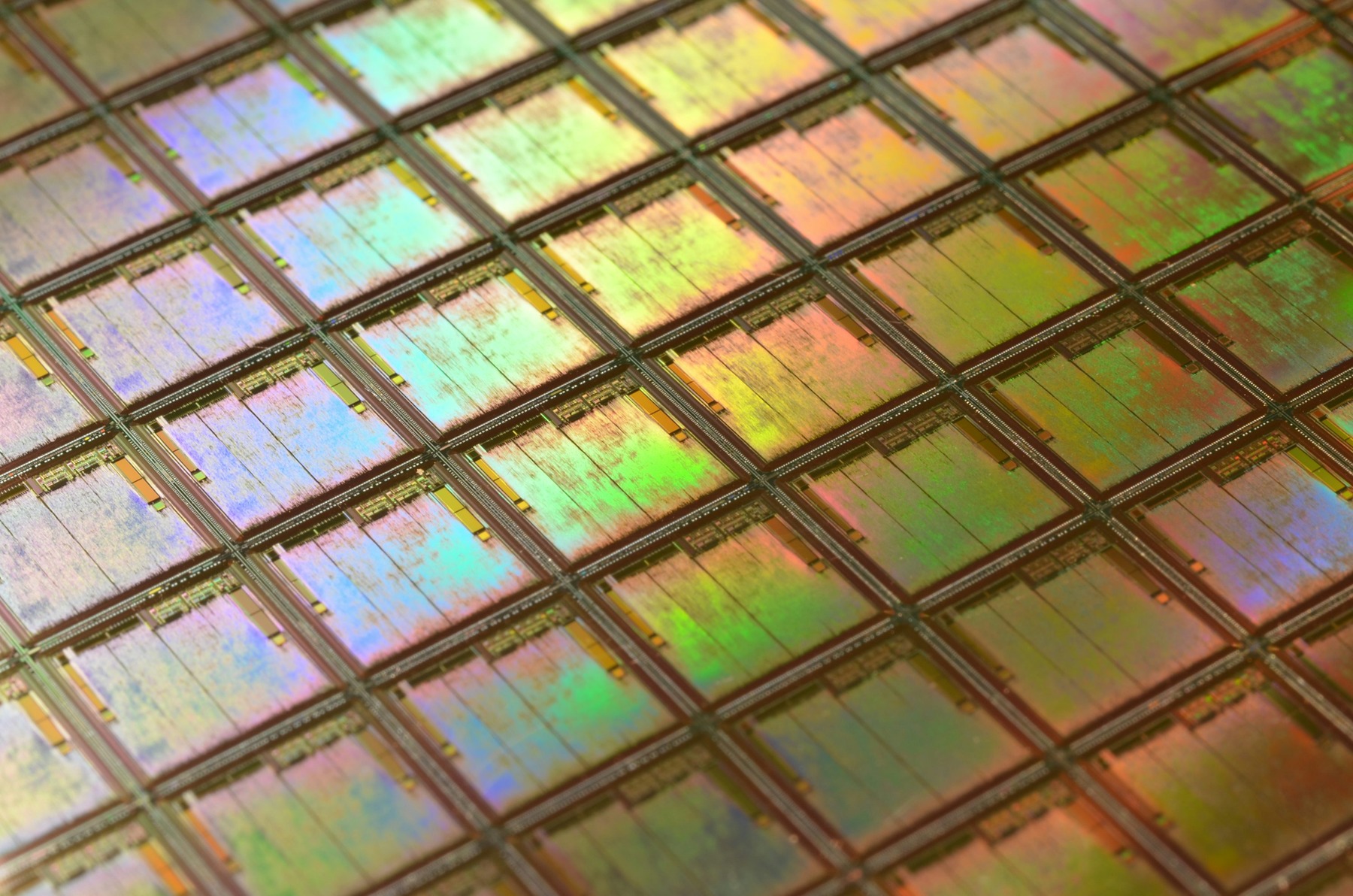
A semiconductor wafer viewed at close range. Illustrative photograph for semiconductor memory technology. Photo: Laura Ockel / Unsplash. Photo source. Free Unsplash licence.