ERS combines three panel-packaging steps in a 310 × 310 mm automated system

Illustrative image: Unsplash contributor on Pexels
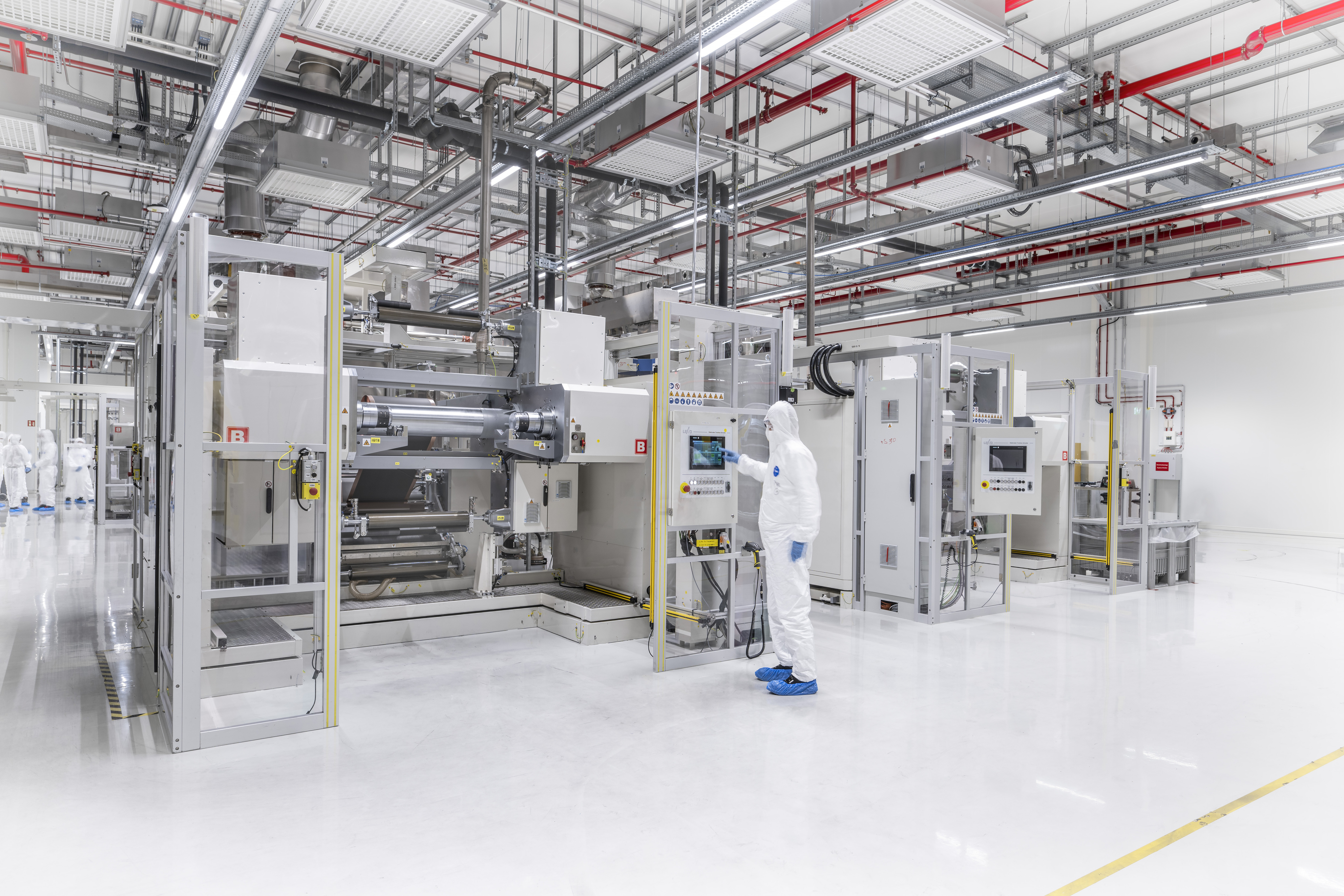
ERS electronic has introduced an automated panel-level packaging system for 310 × 310 mm substrates. The company says the platform combines temporary carrier bonding, debonding and detaping at a throughput of 13 panels per hour.
The first unit has been delivered to an unnamed semiconductor manufacturer for integration into a panel production line. It was developed and manufactured at ERS’s advanced-packaging facility in Barbing, Germany.
Three thermally sensitive steps in one platform
Bonding, debonding and detaping are commonly performed on separate tools. ERS has placed the three processes in one automated system so panels move between internal modules instead of being transferred across the factory floor.
The architecture is intended to reduce handling time and the risk of substrate damage during thermally sensitive processing. It is aimed at dual-carrier workflows associated with backside processing in 3D IC, high-bandwidth memory and 2.5D packaging.
Panel format and throughput
The 310 × 310 mm format offers a larger rectangular processing area than a 300 mm circular wafer, potentially increasing substrate utilisation for suitable package layouts. Real production performance will also depend on warpage, alignment, material compatibility, changeover time and yield.
The quoted throughput and process benefits are ERS figures. The company has not published independent yield data, detailed alignment tolerances or results from the first customer installation.