The efficiency gain is real. So are the wide-bandgap design risks
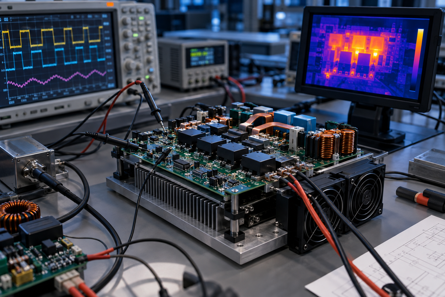
AI-generated illustration: The Electronics Brief
A GaN or SiC device can make a power stage smaller, cooler and more efficient. Put it into a silicon-era layout with an unsuitable driver or slow protection, however, and the headline advantage can disappear in ringing, EMI or device failure.
Wide-bandgap selection is therefore a platform decision. The device, driver, layout, protection, magnetics, cooling and sourcing strategy have to work as one system.
Start with the operating envelope
Silicon carbide MOSFETs are widely considered for higher-voltage, higher-power conversion where switching loss, temperature capability and system size justify the device and drive cost. Gallium nitride devices are attractive for high-frequency conversion where faster switching can reduce magnetic and passive size. GaN and SiC application ranges overlap; neither material alone determines a system’s power rating. The correct choice depends on bus voltage, power, switching frequency, thermal limits, topology, isolation and acceptable EMI.
Comparisons should use the application’s switching conditions. A low headline on-resistance does not capture switching energy, gate charge, output capacitance, reverse conduction or temperature dependence. Compare data at equivalent bus voltage, current, gate drive, temperature and switching conditions. Where datasheet tests differ, use validated models or measurements rather than simply scaling a headline figure.
Gate drive and layout become part of the device
Faster edges reduce switching time but amplify the effect of parasitic inductance and capacitance. Gate-loop and power-loop geometry, return paths, package choice and measurement technique can determine whether the theoretical benefit survives on the board.
The driver must match the device’s voltage limits, gate characteristics and required turn-on and turn-off behaviour. Protection thresholds and dead time may need to change. A probe connection that would be acceptable on a slower silicon design can distort the measurement or introduce enough inductance to mislead the investigation.
EMI and protection need early attention
High dv/dt and di/dt can increase common-mode current, ringing and susceptibility to unintended turn-on. Filtering, shielding and isolation capacitance should be considered with the mechanical layout, not added after the power stage is complete. Short-circuit withstand and fault response also differ between technologies and products; protection timing must be based on the selected device and application. Do not assume that a device has a guaranteed short-circuit withstand time.
Thermal performance is a system question
Lower semiconductor loss does not remove the need for a thermal model. Package thermal resistance, interface material, copper spreading, cooling method and switching frequency all affect junction temperature. Higher power density can concentrate heat even when total loss falls.
Engineers should validate the design across line, load and ambient extremes, including fault and transient conditions. Buyers should confirm package availability, qualification grade, second-source strategy and the supplier’s lifecycle position before the design becomes difficult to change.
Approve the platform, not only the transistor
A credible wide-bandgap decision records the complete power-stage assumptions: device, driver, layout, magnetics, protection, cooling, control and compliance plan. That approach makes the efficiency claim testable and gives sourcing teams a clearer view of which elements are interchangeable and which are tied to the chosen platform.