GaN vs SiC vs silicon MOSFETs: which power device should you choose?

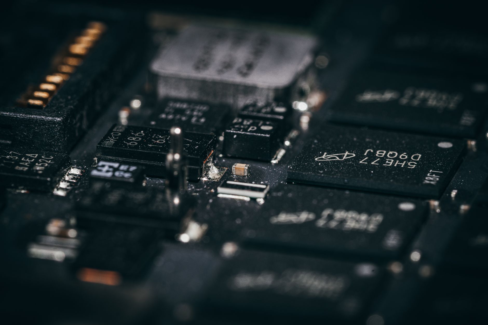
Illustrative image: Unsplash contributor on Pexels
Choosing between silicon, silicon carbide and gallium nitride is not a contest to find the most advanced semiconductor. It is a system design decision.
A faster switch can reduce switching loss and shrink magnetics, but it can also expose weaknesses in the gate drive, PCB layout, insulation system and electromagnetic compatibility. A device with a higher headline rating may add cost without improving the finished converter. A familiar silicon MOSFET may remain the best choice when voltage, frequency and efficiency targets are modest.
The right question is therefore not which material is best. It is which device technology provides the most useful combination of conduction loss, switching loss, voltage capability, thermal performance, controllability, availability and cost in the intended topology.
The short answer
Silicon MOSFETs remain strong at lower voltages and in cost-sensitive designs where established packages, controllers and manufacturing experience matter.
Silicon carbide, usually shortened to SiC, is particularly attractive at higher voltages, high power and elevated temperature. It is widely considered for traction inverters, industrial drives, solar conversion, charging and high-voltage power supplies.
Gallium nitride, or GaN, is attractive where very fast switching and low charge can deliver high power density. Common target applications include compact power adapters, server power supplies, telecoms conversion and other converters where switching frequency and size carry significant value.
These are useful starting positions, not hard boundaries. Improvements in device structure and packaging continue to move the crossover points.
What changes when the semiconductor material changes?
Silicon, SiC and GaN have different material properties, but a designer buys a finished transistor rather than a material table. The practical comparison must be made between real devices at the required voltage, current, temperature and switching conditions.
Wide-bandgap materials allow devices to operate with higher electric fields than silicon. In suitable products this can support higher blocking voltage, lower resistance for a given die area or faster switching. The system benefit may include lower loss, a smaller heatsink, reduced magnetics or higher operating frequency.
Those gains are not automatic. Package inductance, gate-loop layout, reverse conduction, short-circuit behaviour, thermal interface and control strategy can determine how much of the device capability is usable.
Where silicon still makes sense
Silicon MOSFET technology is mature, broadly available and supported by a large choice of drivers, packages and design guidance. At lower voltages, modern silicon devices can offer very low on-resistance at an attractive price.
Silicon is often the rational choice when:
- the bus voltage is comfortably inside an established silicon range;
- switching frequency does not need to rise substantially;
- size and weight are not the dominant constraints;
- the engineering team values proven behaviour and second-source options;
- the cost of changing the gate drive, magnetics, layout and test process outweighs the efficiency gain.
The mistake is to compare a new wide-bandgap device with an old silicon design while leaving the surrounding circuit unchanged. A fair comparison should consider the best credible implementation of each option.
Where SiC earns its place
SiC MOSFETs are frequently selected for high-voltage systems because they can combine high blocking voltage with useful switching performance and high-temperature capability.
At system level, lower switching loss can permit a higher switching frequency. This may reduce the size of inductors, transformers and filters. Lower loss can also reduce cooling demand, although the result depends on the operating point and thermal path.
SiC becomes particularly compelling when a design needs several of the following:
- high DC-link voltage;
- high power throughput;
- high junction-temperature capability;
- reduced switching loss at a frequency where silicon devices struggle;
- reverse-recovery performance suited to the topology;
- a smaller cooling system or passive components.
The design still needs a suitable gate driver, controlled gate-loop inductance, appropriate negative-voltage margin and protection fast enough for the device. Creepage, clearance and insulation requirements continue to be set by the system voltage and applicable standards.
Where GaN changes the design
GaN power transistors can switch extremely quickly. Their low charge and absence of a conventional silicon MOSFET body diode can be valuable in high-frequency conversion, but the implementation must be designed for that speed.
The potential rewards are high efficiency and power density. Faster switching can reduce the energy lost during each transition and allow magnetics to shrink. In a compact adapter or data-centre converter, the saving in volume may be worth more than the difference in transistor price.
GaN is worth serious consideration when:
- the voltage range matches available devices;
- high switching frequency creates a clear system benefit;
- PCB parasitics can be kept tightly controlled;
- the controller and driver can manage the device correctly;
- electromagnetic emissions and common-mode currents will be addressed early;
- the manufacturing process can maintain the required layout and thermal performance.
A very fast edge is not free performance. It can increase ringing, overshoot and electromagnetic interference. Slowing the transition may improve robustness but also surrender some of the efficiency advantage. The optimum design is rarely the fastest possible switching event.
Compare losses at the real operating point
On-resistance is only one part of the loss calculation.
Conduction loss depends on current waveform, duty cycle and resistance at the expected junction temperature. The value at room temperature can understate the loss in service.
Switching loss depends on voltage, current, transition time, device charge, capacitances, switching frequency and the commutation path. Output capacitance energy and reverse-conduction behaviour can be especially important in hard-switched designs.
Gate-drive loss may be small in a high-power converter, but it becomes more visible as frequency rises. Dead time, diode or channel conduction during commutation and the behaviour of the opposing switch also affect the result.
The comparison should use manufacturer data or measured waveforms at conditions close to the application. A figure quoted at a different gate voltage, current or temperature may be useful for screening but not for a final decision.
Packaging can overturn the material comparison
An excellent die in a package with excessive inductance may not deliver the expected switching performance. Equally, a package that provides strong top-side cooling or a low-inductance current path may create a system advantage greater than the difference between two semiconductor materials.
Check:
- source or emitter inductance shared with the gate loop;
- Kelvin-source provision;
- creepage and clearance around the package;
- exposed-pad or top-side cooling requirements;
- whether thermal figures assume a particular PCB construction;
- inspection and assembly capability;
- package availability across more than one device family.
The PCB is part of the switching circuit. Gate driver placement, loop area, current-return path and decoupling must be designed with the selected package rather than copied from a slower device.
Do not ignore fault behaviour
Short-circuit withstand time, avalanche capability, overvoltage tolerance and gate robustness differ between products. A protection scheme developed for a silicon IGBT or MOSFET may not react quickly enough for a wide-bandgap device.
Define the credible fault cases, then verify how the selected part is protected. Desaturation detection, shunt measurement, overcurrent comparators, active gate control and soft turn-off may all be relevant depending on the power level and topology.
The absence of a particular rating in a datasheet should not be interpreted as hidden capability. Ask the manufacturer what behaviour is characterised and what the recommended protection method is.
Make the decision at system level
A useful comparison includes more than transistor price. It should estimate:
- semiconductor and driver cost;
- magnetics and filter changes;
- heatsink, fan or cold-plate implications;
- PCB area and layer requirements;
- EMC mitigation and compliance effort;
- firmware or control changes;
- qualification and manufacturing risk;
- availability and lifecycle support.
The winner may change with production volume. A wide-bandgap device that appears expensive as a line item can reduce the total bill of materials, enclosure size or cooling cost. Conversely, a modest efficiency improvement may not repay a complete redesign.
A practical selection sequence
Start with the required voltage, current, power, topology and environmental limits. Establish realistic efficiency, size and cost targets. Create credible silicon, SiC and GaN implementations rather than comparing bare devices. Model the losses at the expected operating points, then test switching behaviour using the intended package, driver and PCB layout.
Finally, measure the complete converter. Efficiency, thermal behaviour, overshoot and emissions should all be checked across input voltage, output load and temperature.
Silicon, SiC and GaN are overlapping tools. The best choice is the one that improves the finished power system without creating an unmanaged problem elsewhere.
Technical sources
- Infineon, Wide-bandgap semiconductors: SiC and GaN.
- Infineon, SiC modules vs silicon modules: which is the right choice?
- Infineon, What is a GaN FET and how does it work?