PCB processing is moving towards semiconductor-scale tolerances
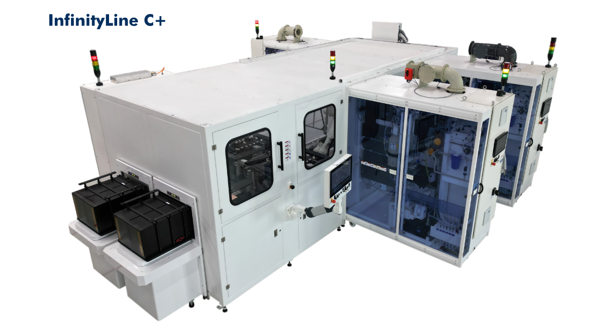
Image: Image: SCHMID Group
The boundary between printed-circuit-board production and semiconductor packaging is narrowing as manufacturers pursue finer conductors, smaller vias and panel-scale integration.
In an interview with I-Connect007, SCHMID vice-president Laurent Nicolet described equipment being developed for embedded-trace substrates, redistribution layers and glass-core packaging.
The company's InfinityLine C+ is a vertical wet-processing cluster in which panels rotate during treatment. SCHMID is targeting approximately 0.8µm vias and 1µm line-and-space features while treating both sides of the panel.
Those dimensions place much greater demands on contamination control, chemistry uniformity and mechanical handling than conventional PCB production.
The panel has become part of the process problem
Nicolet described glass-core thicknesses of between 0.8mm and 1.10mm. Panel-level packaging assemblies, including their carriers, can reach about 6mm thick and weigh between 4kg and 5kg.
Warpage can reach between 4mm and 6mm. A processing system therefore has to transport and support a heavy, distorted panel without damaging the glass or allowing its changing geometry to disrupt the process.
At line widths close to 1µm, a contaminant that would be insignificant on a conventional PCB can obstruct or distort a substantial part of a feature. SCHMID specifies ISO Class 5 operation and filtration down to 0.05µm for the InfinityLine C+.
Glass changes the substrate architecture
Glass offers dimensional stability, a low coefficient of thermal expansion and the potential to create fine through-glass vias. These properties make it attractive for large chiplet assemblies and high-density interposers.
It also introduces new manufacturing steps. Through-glass vias have to be formed, metallised and connected reliably. Adhesion between glass and deposited materials must survive subsequent thermal processing, while panel handling has to account for brittleness and edge damage.
Photoimageable polyimide is also being considered for redistribution layers and embedded-trace structures. Nicolet noted that embedded-trace manufacturing remains at an early stage of industry readiness.
A convergence of disciplines
Advanced packaging now combines problems previously divided between wafer fabrication, PCB production and assembly. Wet chemistry and panel transport must operate at semiconductor-like tolerances, while the substrate remains much larger and mechanically less uniform than a silicon wafer.
The commercial test will be whether those tolerances can be maintained across large panels at a yield and cost suitable for volume chiplet packaging.