PCB stack-up explained: when to use two, four, six or more layers
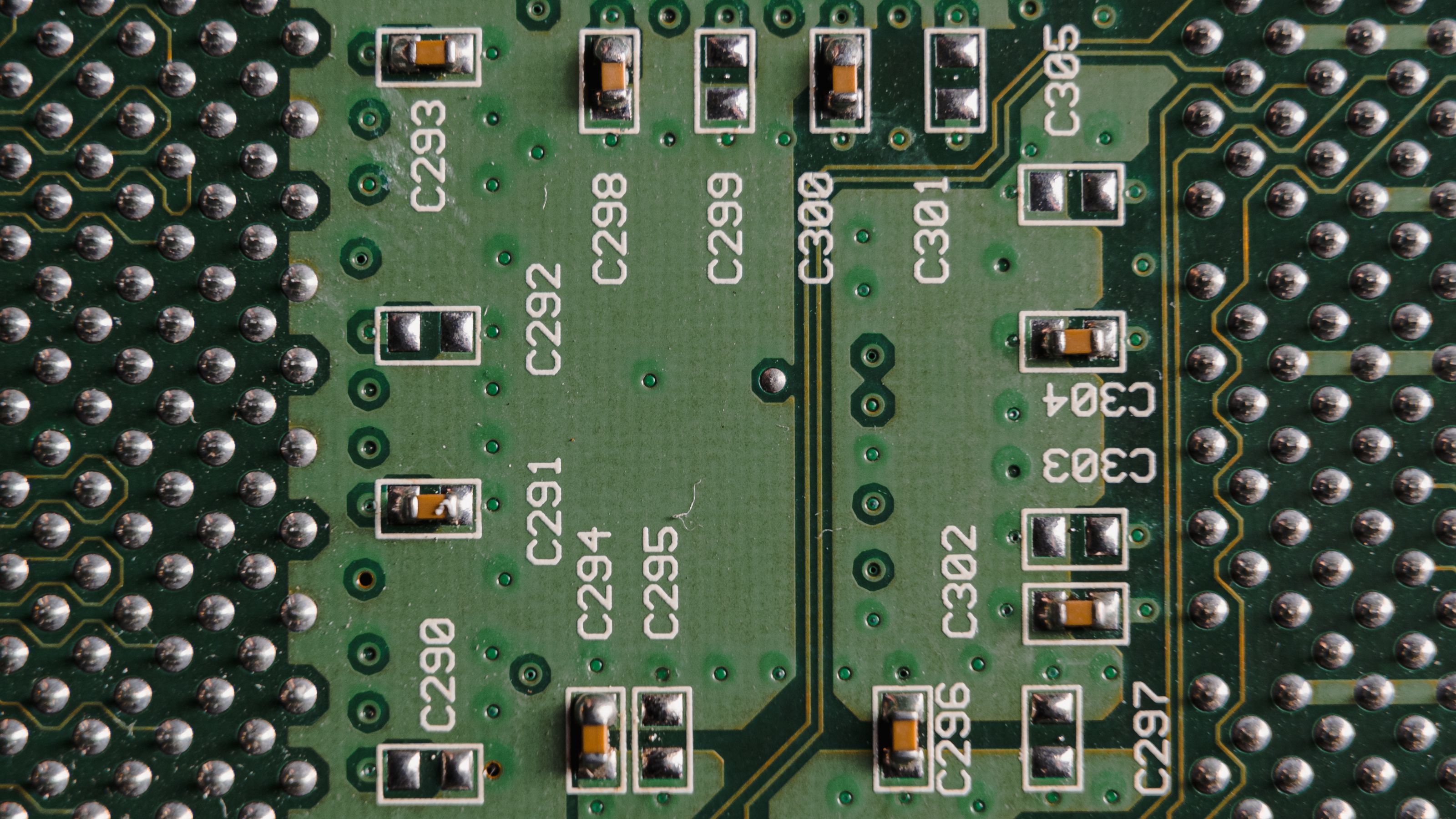
Illustrative image: Unsplash contributor on Pexels
A PCB stack-up is the ordered construction of copper and insulating layers that forms the finished board.
It determines which signal layers sit beside reference planes, how power is distributed and how the fabricator builds the board from copper foil, prepreg and laminate cores. It also affects controlled impedance, electromagnetic compatibility, heat flow, drilling and cost.
Choosing the number of layers only because the tracks fit is therefore a weak design method. A successful stack-up must support the circuit electrically and remain compatible with a repeatable manufacturing process.
Start with the fabricator
The stack-up should be agreed with the intended PCB manufacturer before layout is substantially complete.
Manufacturers hold standard constructions based on materials, copper weights, core thicknesses, prepregs and finished board thickness. Using a proven standard build can improve predictability, shorten engineering review and reduce cost.
Eurocircuits notes that layer sequence, copper thickness and dielectric properties directly affect the electrical behaviour of the PCB, particularly for RF and defined-impedance designs. Its current guidance encourages standardised buildups where these meet the application.
A custom stack-up may be necessary, but it should solve a defined requirement rather than result from arbitrary values entered into the CAD tool.
What is inside a multilayer PCB?
A laminate core is a cured dielectric material with copper on one or both sides. Prepreg contains partially cured resin and bonds layers during lamination under heat and pressure. Outer copper may begin as foil and gain additional thickness during plating.
The final construction therefore depends on:
- copper-layer sequence;
- core and prepreg thicknesses;
- dielectric material and its properties;
- starting and finished copper thickness;
- overall finished thickness;
- drilling and via structure;
- lamination and plating tolerances.
The dielectric constant used for impedance calculations should match the manufacturer's material data and method. A generic FR-4 value is not sufficient for a tightly controlled high-speed design.
When a two-layer PCB is enough
A two-layer board can be entirely appropriate for a simple, low-speed product with modest component density and no demanding power or EMC requirement.
The key limitation is reference continuity. If both layers are heavily routed, signals may have no uninterrupted return plane. Return current then detours around breaks, increasing loop area and coupling.
Two layers work best when one side can retain a substantial ground area and routing is planned to avoid fragmenting it. Keep critical signals short, provide local decoupling and use stitching vias where the return path changes layers.
Moving to four layers may be justified before routing becomes impossible. The gain is often electrical predictability, not simply more track space.
Why four layers are a common baseline
A four-layer stack can provide two signal layers and two internal planes. A familiar arrangement is:
- top signal and components;
- solid ground plane;
- power plane or routed power;
- bottom signal and components.
This can give the top layer a close reference plane and provide low-inductance ground and power distribution. The exact order and spacing matter.
If the bottom signal layer is far from its reference or the power layer is fragmented, it may not receive the same benefit. A power plane is not automatically a valid high-frequency reference if return current must cross splits.
Four layers are often a sensible choice for MCUs, switch-mode supplies, USB and moderate-speed digital systems, provided the layer assignment and return paths are designed deliberately.
What six layers add
Six layers create more options for dedicated ground planes, power distribution and routing while keeping signal layers close to references.
A design with dense BGAs, several power rails or high-speed interfaces may need the additional layers to escape pins and maintain continuous planes. Six layers can also support better separation of noisy power sections and sensitive analogue circuitry without carving the ground system into isolated islands.
There is no single correct six-layer sequence. One arrangement might place signal layers adjacent to ground planes and route power on an internal layer. Another might use a closely coupled power-ground pair. The preferred structure depends on which signals require impedance control, where components sit and how power flows.
Symmetry around the board centre helps reduce warpage and simplifies manufacturing. Copper distribution also matters. An electrically elegant but grossly unbalanced construction can create fabrication difficulties.
When eight or more layers become justified
Higher layer counts are used for complex pin escape, multiple controlled-impedance interfaces, dense power distribution, shielding and large digital systems.
The extra layers can improve design freedom, but they do not automatically improve signal integrity. Poor layer assignment can still create reference changes and resonant plane structures.
Each additional layer affects cost, thickness options and via strategy. Blind, buried and microvias may require sequential lamination and additional process steps. The designer should understand how many press and plating cycles the proposed interconnect structure needs.
High-density interconnect should be selected because the component and routing architecture require it, not because a fine-pitch package appears modern.
Keep every fast signal beside a reference
A high-speed trace and its return current form one circuit. At higher frequencies, the return tends to follow the path of lowest impedance close to the trace on the adjacent reference plane.
When the signal crosses a split, changes reference plane or moves through a via without a nearby return path, the current must find a detour. This increases loop area and can create radiation, crosstalk and discontinuity.
For every critical route, identify:
- its reference layer;
- any plane split or void beneath it;
- what happens when it changes layers;
- where a ground stitching via or return component is needed;
- whether the reference remains valid through connectors.
Do not use labels such as analogue ground and digital ground as a substitute for analysing current paths.
Stack-up and controlled impedance are one decision
Trace impedance depends on geometry and material: trace width and thickness, distance to the reference plane, dielectric properties and, for differential pairs, spacing between traces.
The intended impedance cannot be finalised independently of the stack-up. If the manufacturer changes dielectric thickness, the trace geometry may need to change.
Agree the stack first, then calculate and route using the manufacturer's construction. Specify the required impedance and identify the relevant nets in the fabrication package.
The manufacturer may adjust artwork to compensate for its process. That is one reason a controlled-impedance service and a clear handover are preferable to treating an online calculator as final authority.
Power integrity and plane spacing
Closely spaced power and ground planes add distributed capacitance and can reduce high-frequency impedance, although local decoupling remains necessary.
Plane shapes should follow actual current demand. Narrow necks and fragmented copper can create voltage drop and shared impedance. High-current paths require adequate copper and thermal planning, not simply a layer labelled power.
Switching converters deserve special attention. The high di/dt loops should be compact and kept away from sensitive routing. A solid ground plane helps, but only if the placement and current loop are also correct.
Thermal and mechanical requirements
Copper weight, plane area and thermal vias can spread heat, but the stack-up must connect this heat to a viable path into the enclosure, heatsink or surrounding air.
Board thickness affects stiffness, connector fit and controlled-impedance geometry. Thin constructions may be necessary for a particular connector or flex behaviour. Thick, heavy-copper boards introduce different drilling and plating constraints.
Material glass-transition temperature, decomposition behaviour, coefficient of thermal expansion and loss characteristics may matter in high-temperature, high-frequency or high-reliability applications.
A layer-count decision checklist
Before choosing the board construction, answer:
- Which signals require controlled impedance?
- Which layers will reference them?
- Can reference planes remain continuous?
- How many power rails need low-impedance distribution?
- What fan-out and via structure do the packages require?
- Are creepage, clearance or isolation slots involved?
- What finished thickness and copper weights are needed?
- Is the construction symmetrical and manufacturable?
- Does the fabricator offer a standard stack that meets the requirement?
- What changes if production moves to another approved fabricator?
The stack-up should be a controlled design input, included in the fabrication drawing and revision record. It should not be reconstructed from layer filenames after layout is finished.
Technical sources
- Eurocircuits, What is the buildup of a PCB?
- Eurocircuits, Buildup Editor user guide.
- Eurocircuits, Why standardised buildup.