Controlled impedance PCB design: what engineers need to specify

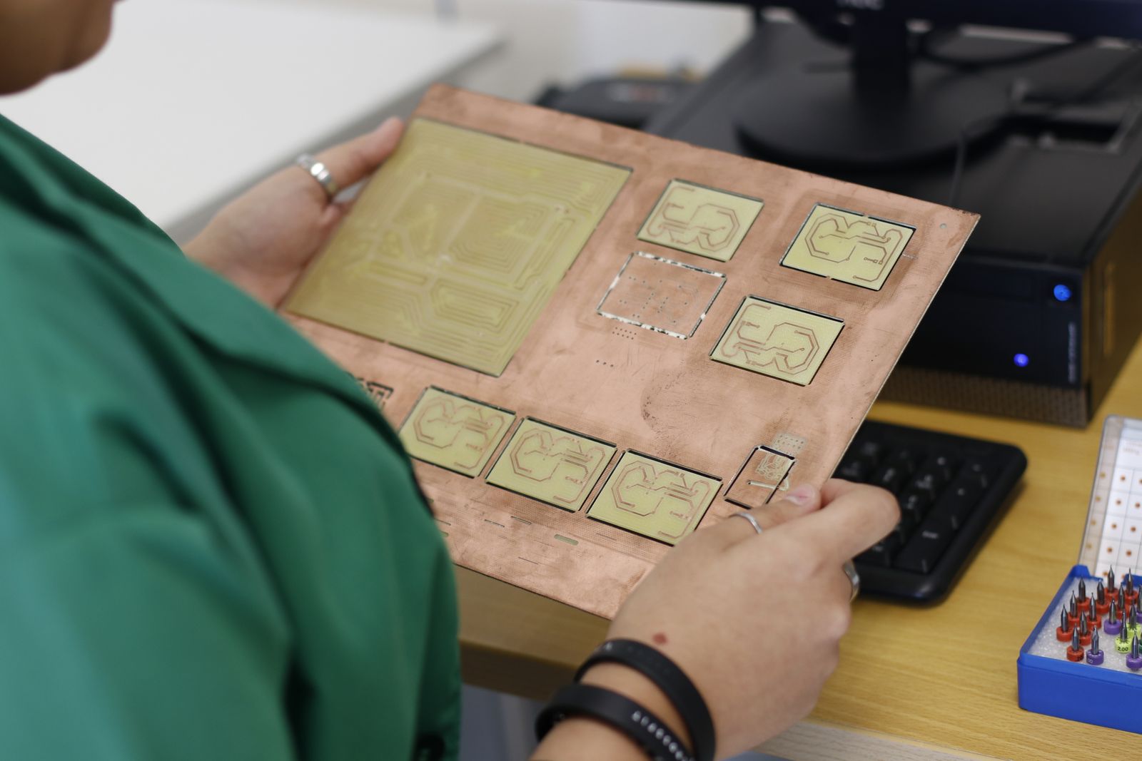
Illustrative image: Unsplash contributor on Pexels
Controlled impedance becomes important when an interconnect behaves as a transmission line rather than an ideal wire.
USB, Ethernet, LVDS, PCI Express, memory buses, RF paths and fast clocks are familiar examples, but the need is driven by signal edge rate, interconnect length and acceptable reflection rather than the interface name alone.
The PCB designer defines a target. The fabricator controls materials and processes that determine the result. Both need a shared, unambiguous specification.
What impedance is being controlled?
Characteristic impedance describes the voltage-to-current relationship of a travelling wave on the transmission line. It depends on the trace and its electromagnetic environment.
For a PCB trace, important variables include:
- trace width and finished copper thickness;
- distance to the reference plane;
- dielectric properties of the material;
- solder-mask effect;
- spacing to neighbouring copper;
- for differential pairs, spacing and coupling between the two traces.
The value cannot be assigned to the trace independently of the stack-up.
Single-ended and differential targets
A single-ended line is specified relative to its reference, commonly 50 ohms in RF and measurement systems.
A differential pair carries opposite-polarity signals. It has a differential impedance determined by each trace's geometry, reference and the coupling between the pair. Common targets include 90 or 100 ohms, depending on the interface.
Do not assume that two independent 50-ohm traces automatically create a 100-ohm differential pair. Pair spacing changes the coupling and therefore the differential value.
The specification should identify whether the target is single-ended, differential or both.
Decide early whether control is required
The threshold at which a route must be treated as a transmission line depends on edge speed and propagation delay. A conservative engineering method compares the signal rise or fall time with the round-trip delay along the interconnect.
If the route is electrically short, reflections may settle before the receiver responds. If it is electrically long, impedance discontinuities, termination and return-path design matter.
Use the fastest credible edge, not merely the clock frequency. A low-frequency control signal driven by modern fast logic can have a demanding edge.
Agree the stack-up before fixing trace widths
Trace width calculators are useful for exploration, but their output depends on input material and geometry. If the fabricator later substitutes a dielectric thickness or material, the calculated width may no longer meet the target.
Ask the manufacturer for a standard controlled-impedance stack-up suitable for the layer count, thickness, copper weight and technology. Eurocircuits, for example, offers defined-impedance constructions and calculates geometry against known material data and controlled processes.
Standard builds are often preferable because their behaviour and process limits are already characterised. A custom stack should be reviewed directly with the fabricator.
Identify every controlled net
Do not rely on the manufacturer recognising interfaces from net names.
Provide a table stating:
- net or class name;
- signal layer;
- reference plane;
- target impedance;
- single-ended or differential requirement;
- tolerance;
- any required test coupon;
- relevant construction or material note.
Use consistent information in the fabrication drawing, CAD rules and data package. Conflicting targets create delay and risk.
Use a realistic tolerance
Impedance varies because material thickness, dielectric properties, copper thickness and etched trace geometry all have tolerances.
A tighter requirement may demand additional control, testing, cost or yield loss. It should be driven by the interface budget rather than selected because a smaller percentage appears better.
Eurocircuits states a typical defined-impedance service tolerance of ±10% for its standardised process. Other manufacturers and specialist services may offer different capabilities. Confirm what the selected supplier can guarantee and how it is verified.
Preserve the reference path
An impedance-controlled trace requires a continuous reference plane. Routing over a split, void or board-edge discontinuity changes the field structure and forces return current to detour.
When a signal changes layer, its reference may also change. Provide a nearby stitching via or appropriate return path so high-frequency current can transfer between reference structures.
Review connectors too. The PCB may maintain impedance up to the pad while the connector launch, cable or via field introduces the dominant discontinuity.
Vias are part of the interconnect
A via adds inductance and capacitance. At high speeds, an unused via stub can create a resonant discontinuity.
Consider:
- via diameter and pad size;
- antipad geometry;
- reference-via placement;
- layer transition;
- residual stub length;
- whether back-drilling, blind vias or another structure is justified.
Differential vias should be laid out symmetrically, but symmetry alone does not guarantee the target impedance. Model or use validated reference structures for demanding links.
Differential-pair matching is not the whole problem
Length matching controls timing skew. It does not repair a poor reference path, excessive loss or a severe impedance discontinuity.
Avoid adding large serpentine structures simply to achieve a cosmetic length match. Closely spaced tuning segments can couple to each other and create different delay from the CAD tool's simple geometric estimate.
Prioritise continuous routing, consistent geometry and the interface's actual skew budget.
Material loss matters as speed rises
At longer distances and higher frequencies, insertion loss can become as important as impedance. Copper roughness, dielectric loss, trace geometry and via structures all contribute.
Standard FR-4 may be adequate for many interfaces, while faster or longer links can justify a lower-loss material. The decision should be based on a channel budget or simulation using material data from the proposed construction.
Changing material can affect cost, availability and lead time. It may also alter impedance geometry, so the complete stack must be revalidated.
How manufacturers verify the result
Controlled-impedance boards may include coupons placed on the production panel. The coupon reproduces relevant layer geometry and is measured, commonly using time-domain reflectometry.
Clarify whether the supplier provides a test report, what tolerance applies and how coupons relate to the board. Coupon success is valuable process evidence but does not prove that every routed feature and connector launch is ideal.
Design review and signal-integrity validation remain necessary where channel performance is critical.
What to put in the fabrication package
Include:
- approved stack-up or reference to the manufacturer's named construction;
- material and finished-thickness requirements;
- finished copper information where relevant;
- controlled-net table;
- target values and tolerances;
- test-coupon and reporting requirements;
- permission and limits for artwork adjustment;
- contact route for technical queries.
Some manufacturers adjust trace widths to compensate for their etching process. Agree whether this is permitted and ensure the final geometry remains compatible with spacing and current requirements.
Review the manufactured system, not only the calculation
For critical interfaces, inspect or measure representative boards. TDR can identify changes along a channel. Eye-diagram, jitter or bit-error measurements can assess the complete link under operating conditions.
Keep the stack-up, impedance report and fabrication revision with the design record. If the supplier, material or construction changes, review the controlled lines before treating the board as equivalent.
Controlled impedance is successful when the electrical target and manufacturing process describe the same physical structure. That agreement begins before routing and ends with evidence from the board that was actually built.
Technical sources
- Eurocircuits, Defining defined impedance.
- Eurocircuits, Defined impedance made simple.
- Eurocircuits, PCB material and track-width tolerance guidance.