Inside Fraunhofer’s plan to wire embedded chiplets as one wafer
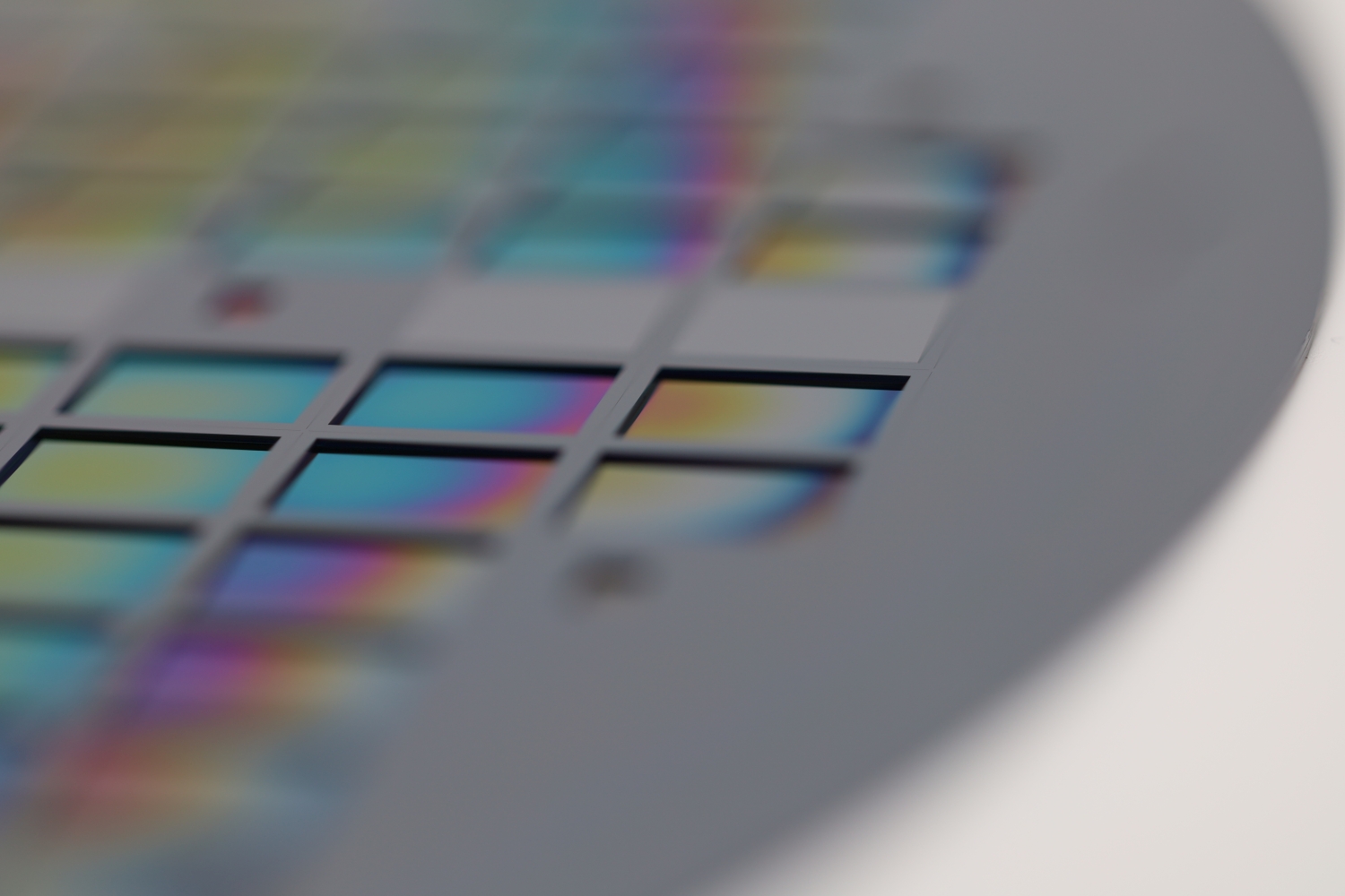
Image: © Fraunhofer IPMS
Fraunhofer IPMS is developing a way to place separately manufactured chiplets into pockets in a silicon wafer, level the surface and connect them through a shared wiring stack. Its quasi-monolithic integration programme, or QMI, aims to combine functions that suit different manufacturing processes without forcing them all into the same silicon recipe.[1][2]
The physical demonstrator uses dummy chiplets, which were inserted into structured recesses before a passivation layer was applied to prepare the surface for subsequent wiring. Fraunhofer announced that milestone on 19 May and revisited it in its November SEMICON Europa preview. The demonstrated work establishes assembly and surface preparation; a functioning circuit built through the complete process remains a subsequent step.[1][3]
A micromechanical sensor needs structures that move or respond to a physical stimulus, while its controller needs transistors and interconnects suited to computation. Building both as separate chiplets preserves those specialised processes, and Fraunhofer’s own QMI process illustration shows a MEMS chiplet integrated with its driver ASIC. The shared wiring then becomes their electrical connection.[2]
Conventional packaging already combines separate dies, often with an interposer carrying signals between them. QMI takes the assembly into a wafer process, where the inserted dies become part of a surface that can receive a common interconnect stack. Fraunhofer is also pursuing 2.5D integration, so this is one route within its wider packaging work rather than a claim that every multichip assembly needs pockets.[2][3]
Once the chiplets are in place, the wiring process inherits their placement and height errors, because each connection has to cross from the surrounding wafer onto an inserted die. The pocket dimensions, placement accuracy and surface preparation have to work together. In an ordinary package, some of that geometry can be accommodated in the package interconnect; here it reaches directly into the common wiring process. [1][2]
Closer connections offer a route to shorter signal paths and a more compact assembly, which is why Fraunhofer identifies sensor AI and high bandwidth transceivers among the intended applications. The published milestone does not yet quantify a system-level speed, energy or yield improvement. Those measurements need an electrically functioning implementation, with the connections carrying real signals between the embedded components.[1][2]
The work belongs to APECS, a European pilot line funded with €730 million over four and a half years to develop advanced packaging and heterogeneous integration. Its scope extends beyond QMI into chiplet design, 2.5D and 3D assembly and the characterisation needed to turn research structures into manufacturable systems. Participating institutions also work with different semiconductor materials, including RF and photonic devices, reflecting how varied the components in a future assembly may be.[4]
Fraunhofer is seeking industrial partners to move QMI into customer applications. In a sensor and controller assembly, the process would have to deliver functioning connections across the wafer and retain them through the finished system’s operating conditions. The research has reached the point of preparing those connections physically, while electrical performance and manufacturing repeatability still need to be established in the customer implementation.[1][2]
Fraunhofer IPMS wafer with placed chiplets from the QMI APECS programme. © Fraunhofer IPMS. Image source. Reuse terms.