Elethron links AlN substrate development to RF fabrication trials

Illustrative image: Laura Ockel on Unsplash
Elethron is developing UK manufacturing of single crystal aluminium nitride substrates, with its AlN4RF programme connecting wafer development to RF processing and packaging. Planned demonstrators include test structures, passive circuits, power modules and active amplifier assemblies, providing different ways to evaluate the material in a fabrication flow.[1][2]
The company cites a bandgap around 6.0 eV and room temperature thermal conductivity of 288 to 316 W/m·K for bulk single crystal AlN. It identifies these as indicative literature values, with variation caused by crystal quality and orientation, rather than specifications for its own wafers.[1]
Turning the crystal into a substrate for epitaxy requires control of defects, orientation, wafer bow and surface finish. Cleaning and high temperature processing can alter the surface before growth, affecting the layers deposited on it and the electrical behaviour of the resulting device. Later contact formation, passivation and packaging add further process requirements, so a useful wafer specification must account for more than the starting crystal.
Elethron plans to develop those specifications with downstream partners, whose intended uses range from RF transitions and interposers to amplifier carriers and III-nitride devices. A carrier beneath an amplifier must move heat while accommodating RF connections, whereas a substrate for epitaxy also needs the crystal structure and surface quality required by the growth process.[1]
For aluminium rich III-nitride layers, native AlN can reduce some of the mismatch associated with a foreign substrate. That offers a route to improved epitaxy, although the deposited layers still have to be characterised and fabricated into devices before any electrical improvement can be established.[1]
Passive structures can reveal RF losses and processing limitations, while active amplifiers add heat flow, contacts and operation under high electric fields. Measurements from both can help identify whether a limitation originates in the substrate, the fabrication process or the assembly, giving the crystal growers specific tolerances to work towards.
Elethron has not published qualified wafer specifications, commercial volumes or delivery dates. Its current plans cover material development and demonstrators leading towards qualification.
Sources
- Elethron, AlN substrate platform, material references and AlN4RF programme
- Elethron, UK single-crystal AlN manufacturing programme
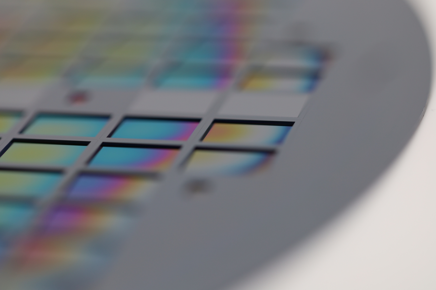
Macro photograph of a patterned silicon wafer, used to illustrate substrate development. The photograph does not show aluminium nitride. Photo: Laura Ockel / Unsplash. Photo source. Free Unsplash licence.