Cognex launches In-Sight 1750 reader for difficult wafer markings
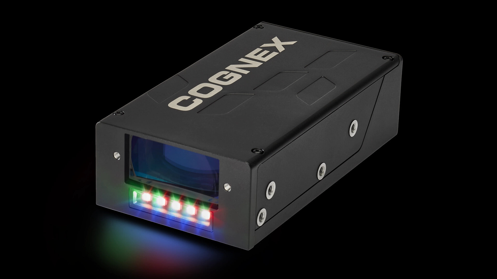
Cognex has launched the In-Sight 1750, a wafer and panel identification system intended to read difficult marks during semiconductor fabrication and packaging.
The company says the system combines imaging, purpose-built illumination and AI-based recognition to identify degraded marks and markings on challenging substrates. It also includes a web-based setup interface and read logging for quality and process-control records.
Traceability is the practical test
A missed identifier can break the link between a physical wafer or panel and its process history. That can lead to manual intervention, delayed equipment cycles and uncertainty over which material has passed through a particular stage. Cognex says the In-Sight 1750 is designed to reduce those interruptions and help manufacturers maintain throughput.
The system is also aimed at existing In-Sight 1740 users. Cognex says job conversion and a straightforward upgrade path should reduce the work needed to move to the new reader. That claim will depend on the installation, interfaces and recipes already in use.
For a production team, the key evidence is not whether the reader uses AI but how it performs on the marks, surfaces and process conditions found on its own line. Buyers should ask for read-rate and false-read data, the range of supported mark types, integration requirements, logging detail and the procedure for handling a failed identification.
Cognex has not published comparative read-rate data or customer results in the announcement. Claims about fewer disruptions and higher equipment utilisation therefore remain supplier claims until tested in the relevant process.