Why Applied and Kioxia are taking memory development into the equipment lab

Illustrative image: TECNIC Bioprocess Solutions on Unsplash
Applied Materials and Kioxia are forming a joint research programme at Applied’s new EPIC Center in Silicon Valley, bringing memory-device development, process equipment and advanced packaging into the same collaborative environment.
The agreement announced on 29 September covers advanced memory-cell structures, new materials, multi-chip stacking and packaging for stacked memory.
It does not identify a product, manufacturing node or commercial launch date. Its significance lies instead in the development model: the equipment supplier and memory manufacturer intend to work alongside one another before new processes reach volume production.
Memory scaling has become a wider systems problem
Kioxia’s core business is flash memory and solid-state storage. Increasing the density and performance of those products no longer depends on one isolated process change.
The cell structure, materials, deposition and removal processes, interconnects and packaging all affect whether a design can be manufactured at useful scale.
Stacking more memory structures can increase capacity without relying entirely on smaller lateral dimensions. It also creates additional requirements around process uniformity, alignment, interconnection, heat and manufacturing yield.
Packaging adds another level. Multiple dies need electrical connections that can deliver the required bandwidth without consuming excessive space or power. The package must also manage mechanical and thermal stresses while remaining suitable for repeatable high-volume assembly.
The Applied and Kioxia programme is intended to work across those boundaries. Its four stated areas are advanced memory-cell and structure creation, multi-chip stacking, advanced packaging for stacked memory and materials engineering that can be transferred into manufacturing.
That is broader than a conventional equipment evaluation. The companies are describing a process in which device requirements and manufacturing technology are developed together.
What the EPIC model is meant to change
Semiconductor development is often sequential. A device maker sets requirements, equipment and materials are developed, individual process steps are tested, and the combined process is then prepared for manufacturing.
A problem discovered late in that sequence can force changes further back through the chain.
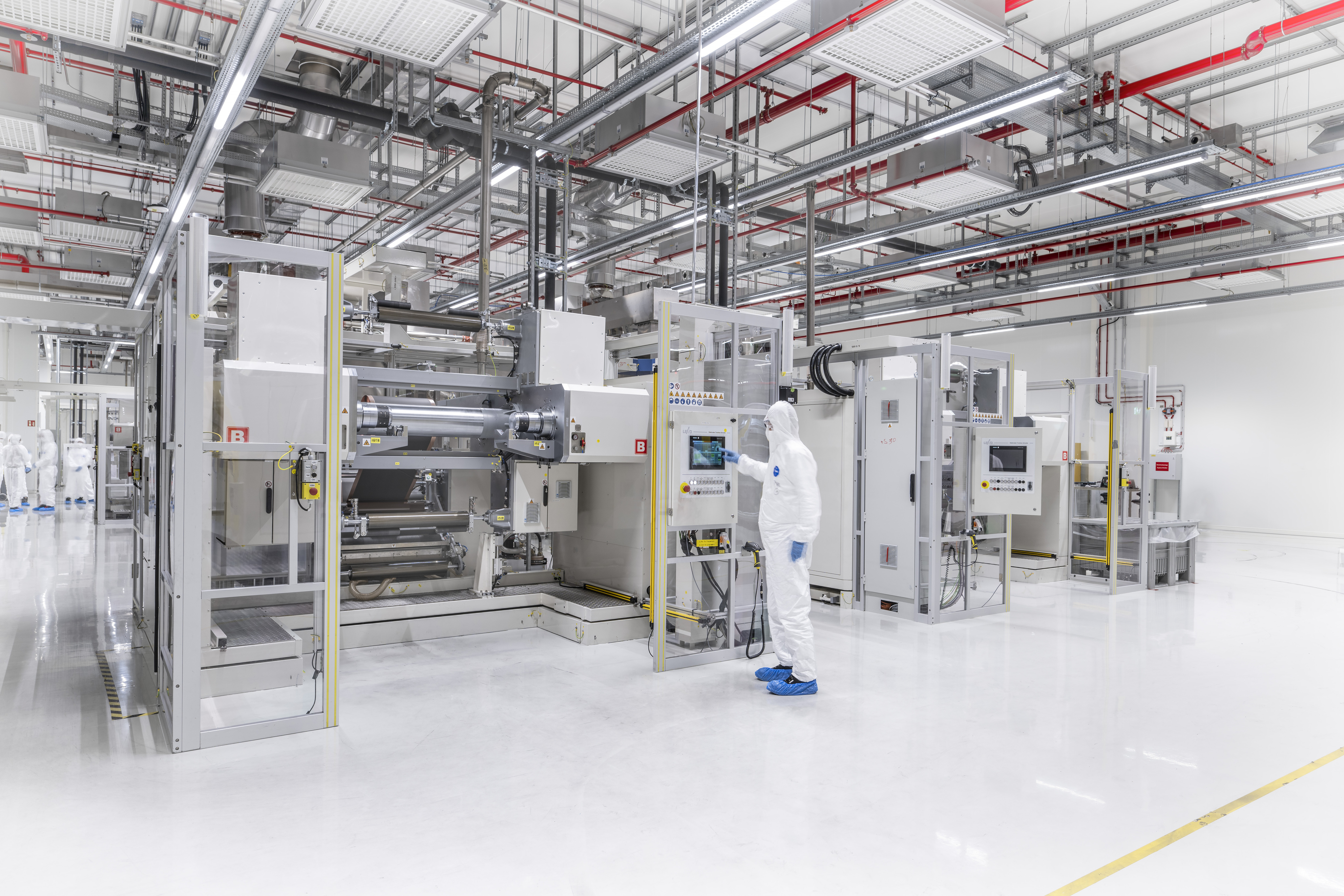
Applied says the EPIC Center is designed to give chipmakers earlier access to its equipment and process-development work. Teams from participating companies will be able to run experiments together and assess interactions between materials, individual process steps and the resulting device structures.
The aim is to shorten the learning cycle between an initial idea and a process suitable for high-volume production.
Applied describes EPIC as a $5 billion investment, although the accompanying note makes clear that capital expenditure is expected to build towards that figure over time as customer projects begin. The company expects the centre to become operationally ready during 2026.
The facility will include a collaborative cleanroom and is being positioned as a meeting point for chipmakers, designers, equipment suppliers and universities.
What the announcement does not establish
There are no stated density, bandwidth, power or endurance targets for the Kioxia programme. Applied and Kioxia have not named a particular NAND generation, stacking format or packaging process.
There is also no timetable for qualification or commercial production.
That limits how far the announcement can be treated as a technology roadmap. It shows where the companies intend to work, but not yet what they have achieved.
The useful evidence will come later: named test vehicles, process results, manufacturing-yield data and a clearer link to Kioxia’s product plans.
For customers and component buyers, this is therefore a longer-term signal rather than an immediate sourcing event. It suggests that future memory development will depend increasingly on closer coordination between device architecture, manufacturing equipment and packaging.
The practical question is whether that coordination produces measurable improvements quickly enough to alter product availability, cost or performance. Until results are published, the partnership is a development route rather than a technical breakthrough in itself.