SUSS enters wafer cleaning with 200mm GT200 platform
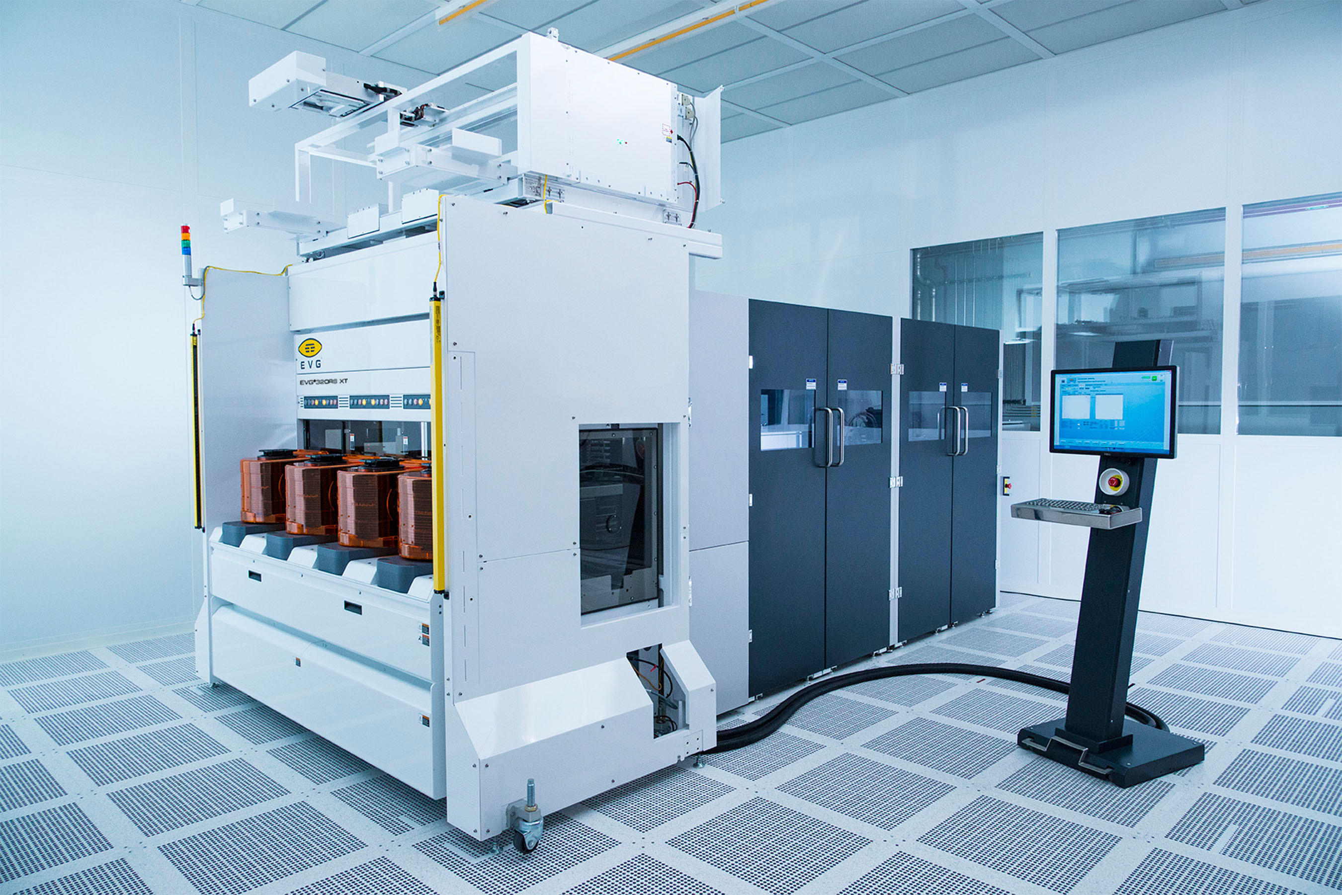
SUSS has entered the wafer-cleaning equipment market with the GreenTec Solutions product line and its first platform, the GT200.
The system is designed for 200mm wafers and supports cleaning, stripping and surface-activation processes. SUSS is targeting research, development and low-volume manufacturing across compound semiconductors, MEMS, advanced packaging and other applications that do not necessarily follow a high-volume silicon process flow.
Wet processing with in-situ ultraviolet treatment
The GT200 combines modular wet-process capability with an in-situ ultraviolet module. UV treatment can alter organic residues and surface chemistry before or after a wet step, depending on the process configuration.
SUSS says the platform is designed to reduce chemical consumption and avoid selected hazardous acids. The announcement does not specify a universal process recipe because cleaning performance depends on the substrate, film stack, contamination and the condition required by the next manufacturing operation.
Residues left after lithography, etching, deposition or temporary bonding can affect adhesion, electrical contact and bonding yield. Compound-semiconductor wafers and MEMS structures can also restrict the chemistries, mechanical forces and drying methods that can be used safely.
A new equipment category for SUSS
SUSS already supplies coating, bonding, lithography and related processing equipment. Adding cleaning places another step within the company's wafer-level process portfolio and creates the option to combine recipes with its existing coating and bonding tools.
The GT200 is described as a low-volume manufacturing system rather than a high-throughput production cluster. SUSS has not yet published throughput, chemical-use figures or comparative particle-removal data in the launch announcement.
The GreenTec line was introduced on 1 October 2026. Further configurations are expected as SUSS develops the product family.