Polishing a semiconductor sample can change the fault being investigated
Aluminium oxide polishing can introduce defects into a semiconductor sample and distort the resistance measurements used to investigate a failing device, according to research reported by AIP.
Thomas Adlmaier and colleagues compared preparation methods for scanning spreading resistance microscopy, which maps local electrical resistance. Samples polished with aluminium oxide showed elevated resistance. Embedding samples in epoxy resin and polishing with diamond avoided the errors observed in the study.
The preparation process introduced traces of copper, which interacted with dopants. That explained part of the effect, but the researchers could not account for the full spread of results. Hydrogen associated with humidity during storage is another suspected contributor.
“Every time I thought I understood what’s happening, I was wrong,” Adlmaier said.
The team also found that annealing at 150°C for 15 minutes could reverse much of the preparation damage under the conditions studied. The underlying mechanism remains unresolved: the same measurement intended to reveal a device defect can therefore include a contribution from preparing the sample.
Sources
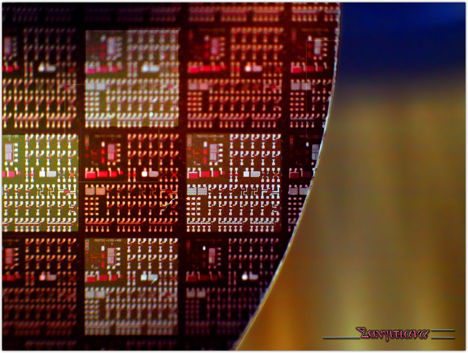
Image: Semiconductor wafer. Illustrative image, not a sample from the study. Sangitiana Fararano. Image source. CC BY-SA 2.0.