Keysight brings Tower’s silicon photonics process into ADS
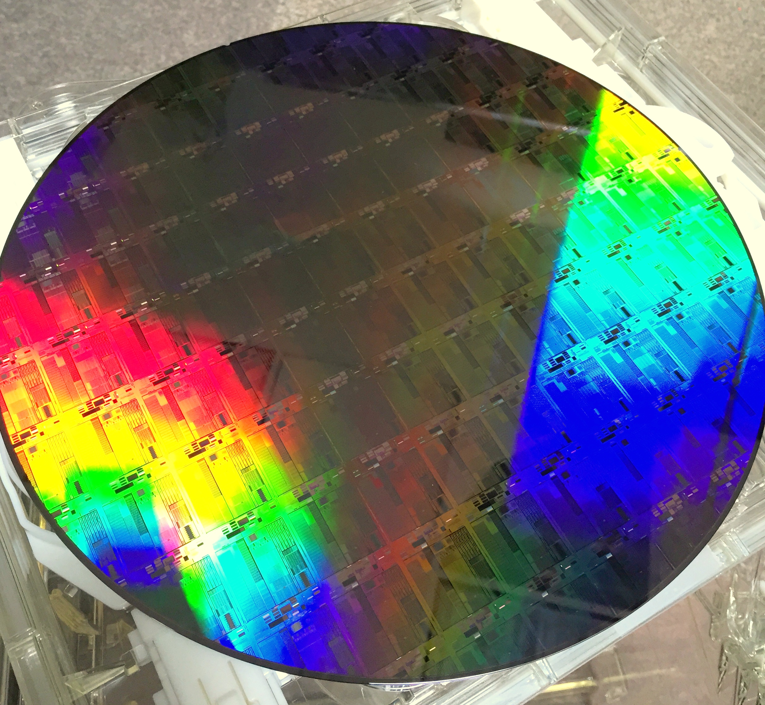
Illustrative silicon photonics wafer. Ehsanshahoseini / Wikimedia Commons · CC BY-SA 4.0
Keysight has certified ADS Photonic Designer to support Tower Semiconductor’s PH18 silicon photonics process design kit, which is now available. Designers can bring the foundry’s photonic device models into the same ADS schematic as the electronic circuits that drive and receive the optical signal. The announcement extends an existing relationship: Tower’s RF processes have been supported in ADS for more than a decade.
Consider the path through an optical transmitter and receiver. A driver applies an electrical signal to a modulator, which encodes it onto light. At the receiver, a photodetector turns the optical signal back into an electrical one that the front end must recover. The stages can be designed separately, but their interactions matter. The drive waveform changes what the modulator sees and the detector’s response influences what the receiver has to work with. The PH18 kit supplies physics-based component models so those interfaces can be considered together in an electrical-to-optical-to-electrical simulation.
The integration also extends to layout. ADS provides photonic layout elements designed to comply with process rules and can compare the layout with the schematic during design. That gives a team a way to catch discrepancies while it is still working in ADS. Tower’s own tools remain responsible for foundry-level verification and tapeout, so the new workflow changes where the design is assembled and checked during development while leaving final sign-off with the foundry.
Sources: Keysight newsroom, 9 November announcement; Keysight’s full Business Wire release, syndicated by MarketScreener.