How a 22.9 µW zoom ADC eases the load on its signal source
A continuous-time zoom ADC described in A-SSCC research combines a capacitive input with coarse and fine conversion paths, reporting 87.5 dB signal-to-noise-and-distortion ratio across a 20 kHz bandwidth at 22.9 µW. The 65 nm prototype operates from 1.2 V, accepts a 2.4 V peak-to-peak differential full-scale input and reports input impedance above 5.6 MΩ. [1]
The input interface deserves as much attention as the conversion result. A low-power converter can leave a substantial system-level bill if its source needs a power-hungry amplifier simply to drive it.
Why the driver can outweigh the converter
In a conventional switched-capacitor input, connecting the sampling capacitor draws a transient current from the source. The source and any driver must restore the required voltage within the acquisition interval. Analog Devices describes how that kickback creates bandwidth and slew-rate demands which can make the input buffer more complicated than the ADC’s power number suggests. [2]
Filtering pulls in the other direction. Reducing analogue bandwidth rejects unwanted signals and noise, whereas settling a charging transient quickly favours a fast driver. The component values and amplifier therefore have to satisfy both jobs together. A resistor chosen solely to improve filtering can also slow the charge transfer that establishes the sampled voltage.
Continuous-time conversion changes that interface, although it does not automatically make every such converter suitable for a high-impedance sensor. Analog Devices’ CTSD architecture, for example, presents a resistive input. Removing switched-capacitor kickback simplifies the drive problem, but the source still has to supply the current demanded by that resistance. [2]
Two paths share the conversion
A zoom converter first locates the input approximately with a coarse converter, then uses a fine delta-sigma path to resolve the smaller remaining range. That division can save energy, because the fine stage does not need to handle the entire input span with the same precision. TU Delft’s published account of the architecture also identifies the complications, including leakage of coarse quantisation noise into the signal band and overload from large out-of-band signals. [3]
The new prototype uses a continuous-time noise-shaping SAR in the coarse path and a Gm-C delta-sigma converter in the fine path. Its coarse noise shaping suppresses quantisation-noise leakage and shapes gain error between the separate DAC paths. The authors also report more than 58 dB alias rejection. [1]
Dividing the reported power by the supply gives about 19 µA, a calculation for the ADC’s reported operating point rather than a complete sensor node. A bridge, reference, bias network or processor could each alter the total substantially. Similarly, a high input impedance does not remove input leakage, parasitic capacitance or board contamination from an actual sensor interface.
The available author abstract does not supply a complete input-impedance curve, reference budget or large-interferer test matrix. Those details would determine how far the simplified front end can be taken in a real circuit, especially when the source impedance varies with frequency.
Sources
- A-SSCC, author abstract for the 22.9 µW capacitive-input CT zoom ADC, paper 1239
- Analog Devices, CTSD input and reference drive requirements (background)
- TU Delft, The Zoom ADC: An Evolving Architecture, 2023 (architectural background)
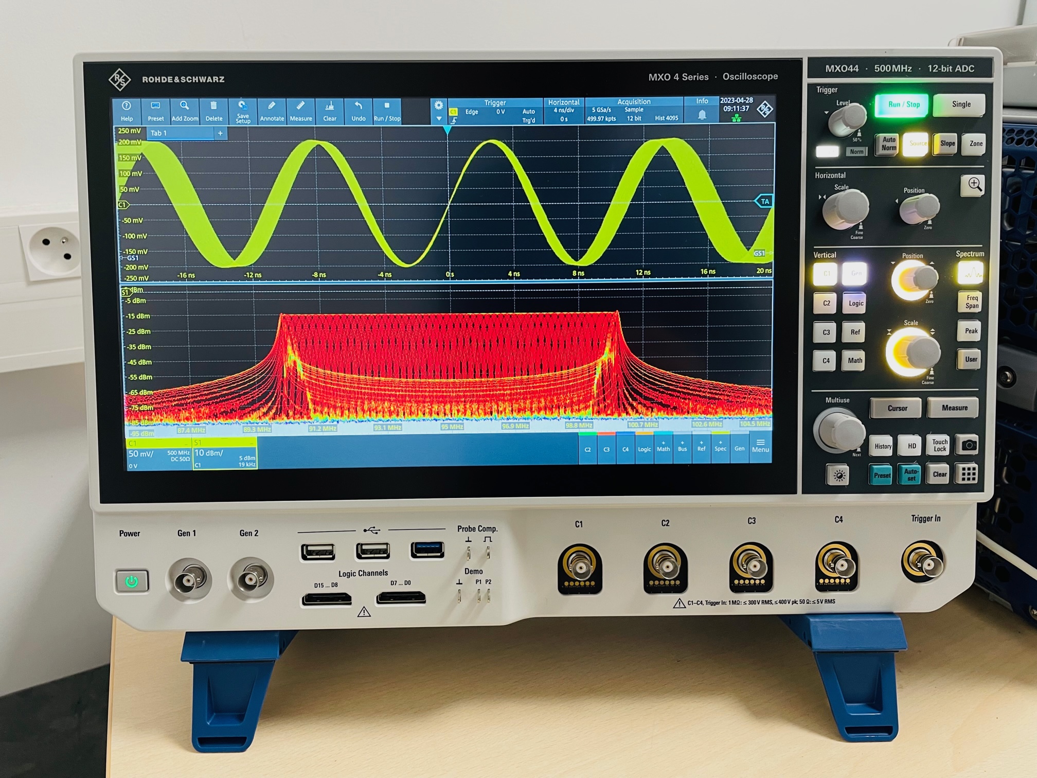
Image: Illustrative signal measurement photograph, not a measurement of the research ADC. Original image unmodified; CC BY-SA 4.0 applies to the photograph. Credit: Wilson Monse / Wikimedia Commons. Image source. CC BY-SA 4.0.