Decoupling capacitors explained: value, placement and common mistakes
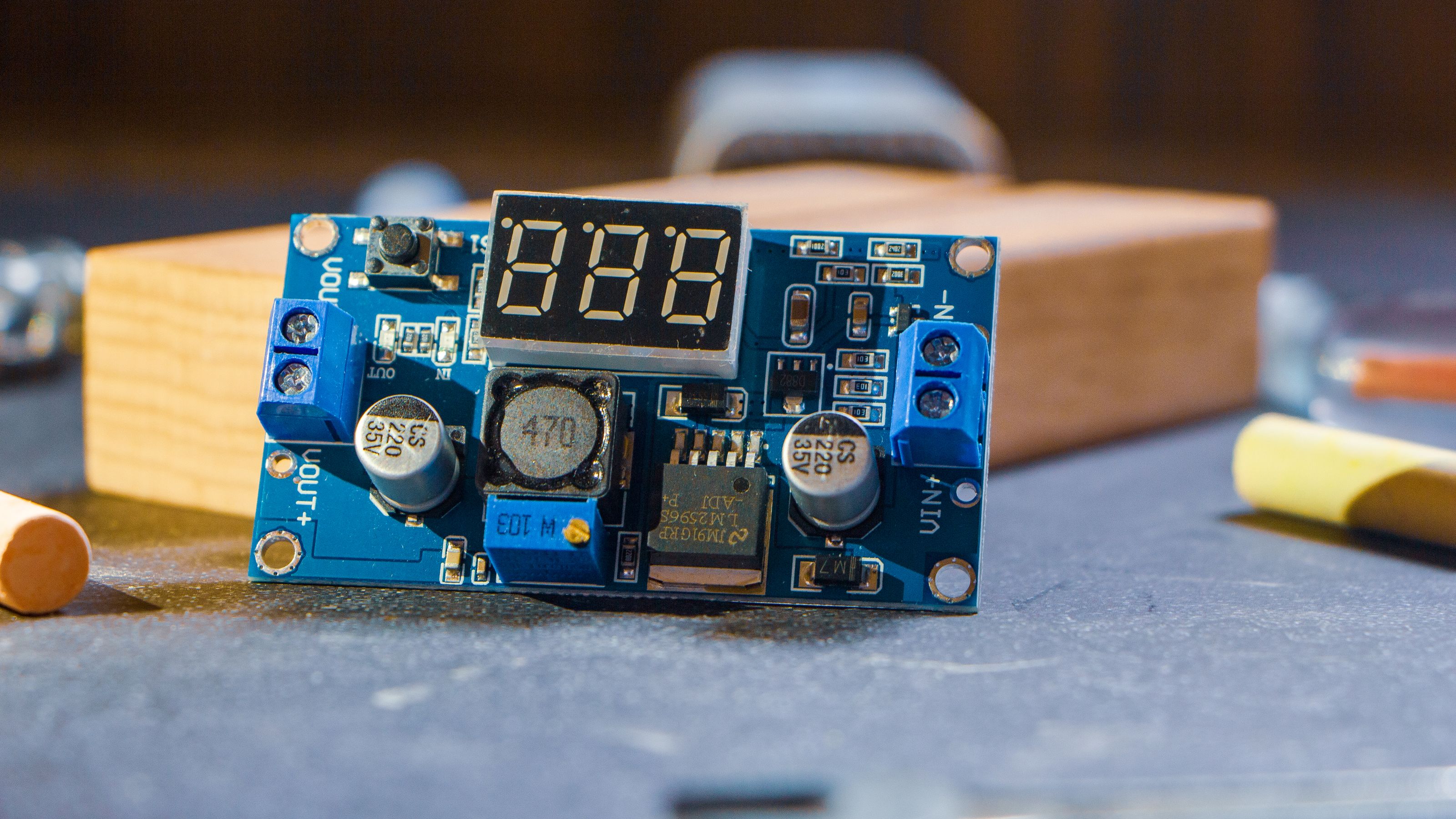
Illustrative image: Unsplash contributor on Pexels
An integrated circuit draws current in short bursts as internal transistors switch. The regulator and bulk supply may be too far away, electrically, to provide that current without a temporary drop in supply voltage.
A decoupling capacitor provides a local charge reservoir and helps keep the impedance of the power-distribution network low over a useful frequency range. It also gives high-frequency current a compact path between the device's supply and return pins.
The familiar instruction to place a 100 nF capacitor near each supply pin is a reasonable starting habit. It is not a complete power-integrity design.
Decoupling, bypassing and bulk capacitance
The terms decoupling and bypass are often used interchangeably. Both describe using capacitance to reduce unwanted voltage variation and provide a low-impedance high-frequency path.
Bulk capacitors support slower load changes and provide energy across a larger part of the board. Local high-frequency capacitors respond to faster current demand close to an IC. Mid-frequency requirements may be shared between several values, package sizes and the plane structure.
These roles overlap. The useful distinction is not the label but the frequency range, current loop and location each part serves.
The capacitor is not ideal
A real capacitor includes capacitance, equivalent series resistance and equivalent series inductance.
At lower frequencies, its impedance falls as frequency rises. Around self-resonance, capacitance and inductance balance and impedance is low. Above self-resonance, parasitic inductance dominates and impedance rises.
Package size, termination geometry, mounting and vias all influence inductance. A physically smaller capacitor can remain effective to a higher frequency even if its nominal capacitance is lower.
This is why a list of values is not enough. The installed impedance of the network matters.
Why placement matters
Transient current flows in a loop from the capacitor to the IC supply pin, through the device and back to the capacitor ground terminal. Inductance increases with loop area and conductor length.
The objective is to keep that loop short, wide and close to the relevant pins or planes.
Useful layout practices include:
- place the local capacitor on the same side as the device where practical;
- minimise the distance between capacitor pads and supply or ground connections;
- use short, wide connections;
- place vias immediately beside or within the capacitor pads where the design rules allow;
- avoid routing through a long narrow neck before reaching the capacitor;
- connect to solid reference planes rather than fragmented copper.
TI hardware guidance repeatedly emphasises keeping bypass capacitors close to device pins and minimising the inductance of their connections.
Route through the capacitor or connect to planes?
For some devices, the preferred arrangement routes the supply into the capacitor and then into the IC pin. This can force the high-frequency path through the local component.
For dense BGAs and plane-fed rails, capacitor and device may instead connect into closely spaced power and ground planes through short vias. The plane pair and via geometry become part of the loop.
Follow the device manufacturer's reference layout where one is provided. A general rule should not override a validated package-specific design.
Choosing the nominal value
The required charge for a transient can be approximated from:
C = I × Δt ÷ ΔV
where I is the current step, Δt its duration and ΔV the permitted voltage change.
This calculation can indicate scale, but it assumes an ideal capacitor and ignores the power network. At fast edges, inductance may dominate before the nominal capacitance can respond.
Use the device datasheet or hardware guide as the primary starting point. It may specify particular values, quantities, locations and dielectric types for each power domain.
Effective capacitance can be far below the label
Multilayer ceramic capacitors using Class 2 dielectrics can lose substantial capacitance under DC bias. Package size, voltage rating, dielectric and manufacturer all influence the result.
A 10 µF capacitor measured at a small AC test signal may provide only a fraction of that value at its operating voltage.
Check manufacturer bias curves or models at the intended voltage and temperature. Allow for tolerance and ageing. Where capacitance is critical, compare effective rather than nominal values.
Why several values are used
Designers often place a small capacitor for high-frequency behaviour, a larger local capacitor for lower-frequency current and bulk capacitance near the regulator or connector.
This can create a broad low-impedance network, but arbitrary value decades such as 100 pF, 1 nF, 10 nF and 100 nF are not automatically optimal. Interactions between capacitance and inductance can create anti-resonant peaks with higher impedance than either component alone.
Modern designs increasingly use simulation or impedance measurement to evaluate the network. Manufacturer reference designs provide an important starting point for complex processors and FPGAs.
Power and ground planes help, but do not replace local parts
Closely spaced planes add distributed capacitance and provide a low-inductance current path over part of the frequency range. They can also spread current between several local capacitors.
Their performance depends on spacing, dielectric and geometry. A plane split or narrow connection can introduce impedance. Local decoupling is still needed at devices with fast transient demand.
The stack-up should be chosen with power integrity in mind. Placing power and ground planes close together can be more useful than separating them by a thick core.
Common mistake 1: the capacitor is close in the schematic only
Schematic symbols contain no physical distance. A capacitor drawn beside an IC may sit several centimetres away after placement.
Assign placement constraints and review the actual current loop. Do not leave decoupling placement until the routing is complete.
Common mistake 2: long via and trace loops
A capacitor may appear close in plan view while its ground connection travels through a long trace or remote via. Both terminals need a short path.
Avoid daisy-chaining several capacitors through one narrow connection unless the arrangement has been analysed for the relevant frequencies.
Common mistake 3: using the wrong return
Connecting the capacitor to an isolated copper island or a plane that is not the IC's high-frequency reference can make the loop unexpectedly large.
Power-domain and ground-domain boundaries need deliberate treatment. Where isolation is required, use the manufacturer-recommended arrangement for each side of the barrier.
Common mistake 4: ignoring regulator stability
Output capacitors around regulators are not interchangeable generic decouplers. Their capacitance, ESR and placement may be part of the control-loop stability requirement.
Follow the regulator datasheet across voltage, bias and temperature. Adding or removing capacitance can change transient response or stability.
Common mistake 5: measuring with a long probe ground
A long oscilloscope ground lead can show ringing created by the measurement loop.
Use a short ground spring, coaxial connection or suitable power-rail probe. Measure at the device pins or designated point with enough bandwidth and dynamic range to see the relevant event.
Record the measurement connection because it forms part of the result.
A practical design process
- Identify each power domain and its permitted ripple or transient range.
- Follow device-specific capacitor recommendations.
- Check effective capacitance at operating voltage and temperature.
- Select the stack-up and plane arrangement.
- Place critical capacitors before general routing.
- Review the physical current loop for every high-demand pin or domain.
- Simulate or estimate power-network impedance where complexity justifies it.
- Measure representative hardware during start-up and worst-case activity.
The goal is not the largest possible capacitor bank. It is a controlled power network with sufficiently low impedance over the frequencies where the load demands current.
Technical sources
- Texas Instruments, hardware design guidance covering decoupling selection and placement.
- Texas Instruments, Decoupling capacitors training on PCB path length, vias and parasitics.
- Device-specific manufacturer hardware-design and reference-layout documentation.