Can a compliant thermal interface solve warped AI packages?
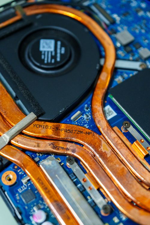
Illustrative image: Unsplash contributor on Pexels
NovoLINC says its MaxLINC thermal-interface material transferred 3.3kW from a production-representative silicon test die while accommodating approximately 150µm of warpage.
The company reports a uniform heat flux of 400W/cm² and a junction temperature below 90°C throughout the demonstration. The result addresses a problem that becomes more difficult as AI accelerator packages grow larger and dissipate several kilowatts.
Why warpage matters
A cold plate or heat spreader cannot remove heat effectively unless it maintains a low-resistance path across the active area of the package. A large silicon die, package substrate and surrounding materials expand by different amounts during assembly and operation.
The resulting bow or local height variation prevents two nominally flat surfaces from touching uniformly. Pressure concentrates at the highest points, while microscopic or visible gaps remain elsewhere. Those gaps can raise local thermal resistance and create hot spots even if average package temperature appears acceptable.
A conventional thermal grease can fill small surface irregularities but may be displaced under repeated thermal cycling. A solid pad can provide controlled thickness but may require enough pressure to threaten the package or its interconnects. Phase-change and liquid-metal materials introduce different handling, compatibility and reliability considerations.
What NovoLINC tested
NovoLINC describes MaxLINC as a compliant thermal interface designed to follow a warped surface while maintaining contact under load. In the reported test, the silicon die had about 150µm of warpage and was operated at a total power of 3.3kW.
The quoted 400W/cm² is a uniform applied heat flux. Real processors do not normally dissipate power uniformly: compute blocks, memory interfaces and disabled regions produce a spatial map that changes with workload. Local heat flux may therefore differ from the average value used in a test vehicle.
The company also reports keeping the simulated junction below 90°C. Interpreting that result requires the inlet coolant temperature, flow rate, cold-plate construction, interface thickness, applied pressure and temperature-measurement method. These details were not all provided in the announcement.
Compliance is only one part of qualification
A compliant interface can reduce the pressure needed to make contact across a bowed package, but long-term qualification must establish whether that contact survives.
Relevant mechanisms include pump-out, dry-out, mechanical creep, compression set and movement during power cycling. The material must also remain chemically compatible with the lid or exposed silicon, cold plate and any sealing or retention materials.
Package assembly tolerances matter alongside intrinsic thermal conductivity. A very conductive material can still perform poorly if it leaves voids or requires an unrealistic mounting load. Conversely, a slightly less conductive interface can provide lower overall resistance if it maintains a thinner and more uniform bond line.
What the demonstration establishes
The test shows that MaxLINC can operate at a power and warpage level representative of emerging multi-kilowatt accelerators under NovoLINC's stated conditions. It does not yet provide a complete production qualification.
Comparative data against established interface materials, thermal-cycling results, pressure maps and ageing measurements would show whether the initial performance is sustained. System developers will also need package-specific data because die area, lid construction, fastener pattern and cold-plate stiffness alter the mechanical problem.
NovoLINC announced MaxLINC in September 2026 and disclosed the 3.3kW warped-silicon demonstration on 6 October.