Siemens builds a virtual golden board for PCB inspection
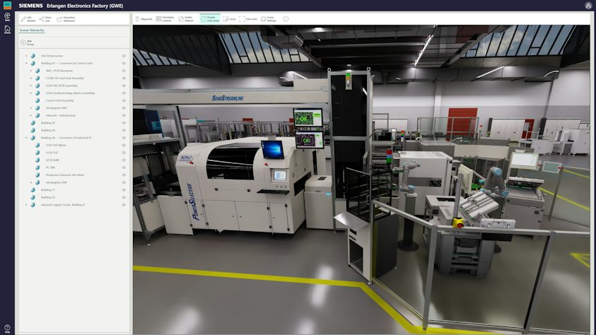
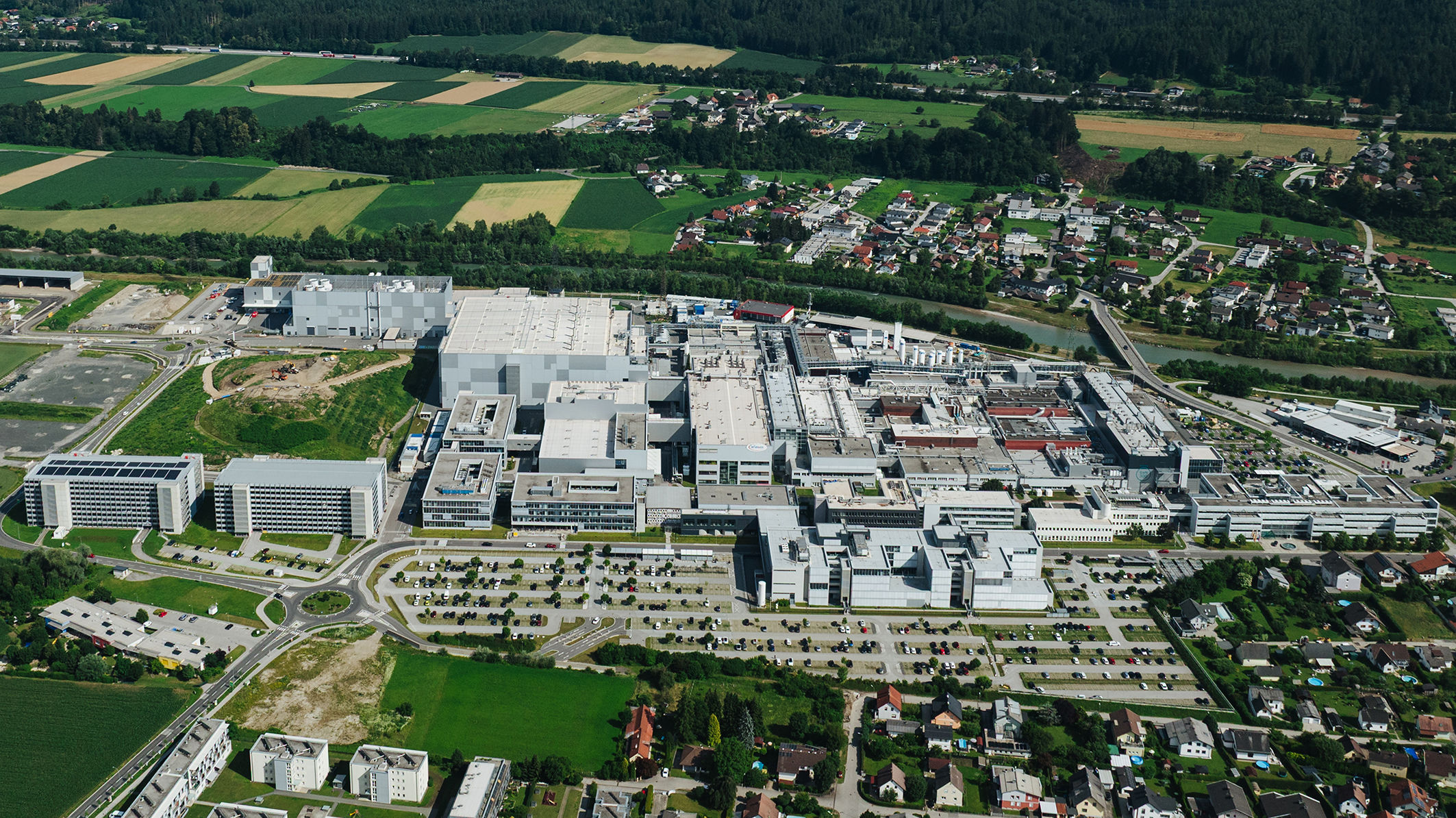
Siemens and NVIDIA are preparing automated optical inspection before the first physical PCB assembly reaches the line. Their demonstration at Siemens’ Erlangen factory uses a virtual golden board to generate images of good assemblies and manufacturing defects.
“Manufacturers shouldn’t have to wait for the first physical circuit board to start preparing inspection,” says NVIDIA’s Rev Lebaredian. The proposed workflow starts with engineering information that already exists: the board design, its bill of materials and the component descriptions. Siemens’ Process Preparation X assembles those inputs into a digital PCBA, and NVIDIA Cosmos generates the inspection images.
The proposed inspection data path
- Teamcenter: PCB design, bill of materials and component information
- Process Preparation X: Validated product data and a digital representation of the assembly
- NVIDIA Cosmos: Synthetic images representing good and defective assemblies
- Secondary inspection: Assessment of conditions flagged by AOI during production
A substitute part can fit the same footprint and perform the same electrical function while having a different body, surface finish or marking. Those visible differences belong in the reference used by the camera system. An accurate netlist alone cannot supply them. Process Preparation already handles component libraries, inspection outputs and product revisions. Bringing image generation into that chain gives the virtual board a route back to the actual assembly data. It also makes a revision error consequential: the inspection system could be trained on an appearance that no longer matches the approved part.
Generating defective examples offers another advantage. A physical board contains the faults that happened to occur; a generated dataset can deliberately explore a wider range. The difficult part is preserving the geometry of the fault while varying lighting, camera position and surface appearance. A solder bridge still has to look like a solder bridge after the image has been made more photorealistic.
At Erlangen, Siemens is also demonstrating AI assistance in the examination of the potential defects flagged by AOI. This provides a second use of the system once physical boards are in production: reducing the number of acceptable assemblies sent for manual review.
Siemens and NVIDIA are targeting up to 85% less manual effort in AOI programme generation, around 40% fewer false calls and more than 5% improvement in first pass yield.