Samsung aims to cut semiconductor materials development from five years to two
Samsung wants AI to shorten the development of new semiconductor materials from five years to two, while identifying more than five times as many promising candidates. Choi Young-sang, an official at the Samsung Advanced Institute of Technology, outlined the targets at an industry forum on 26 October. Samsung also aims to reduce the experiments needed to establish optimal conditions by more than 80%, according to Yonhap’s report.
The scale of the search is considerable. Choi said a semiconductor structure with seven layers can present more than 100 million material combinations, against a research capacity of roughly 50 experiments a month. He also pointed to information that is routinely left unused: “Data from failed experiments also has not been fully utilized.”
Sources
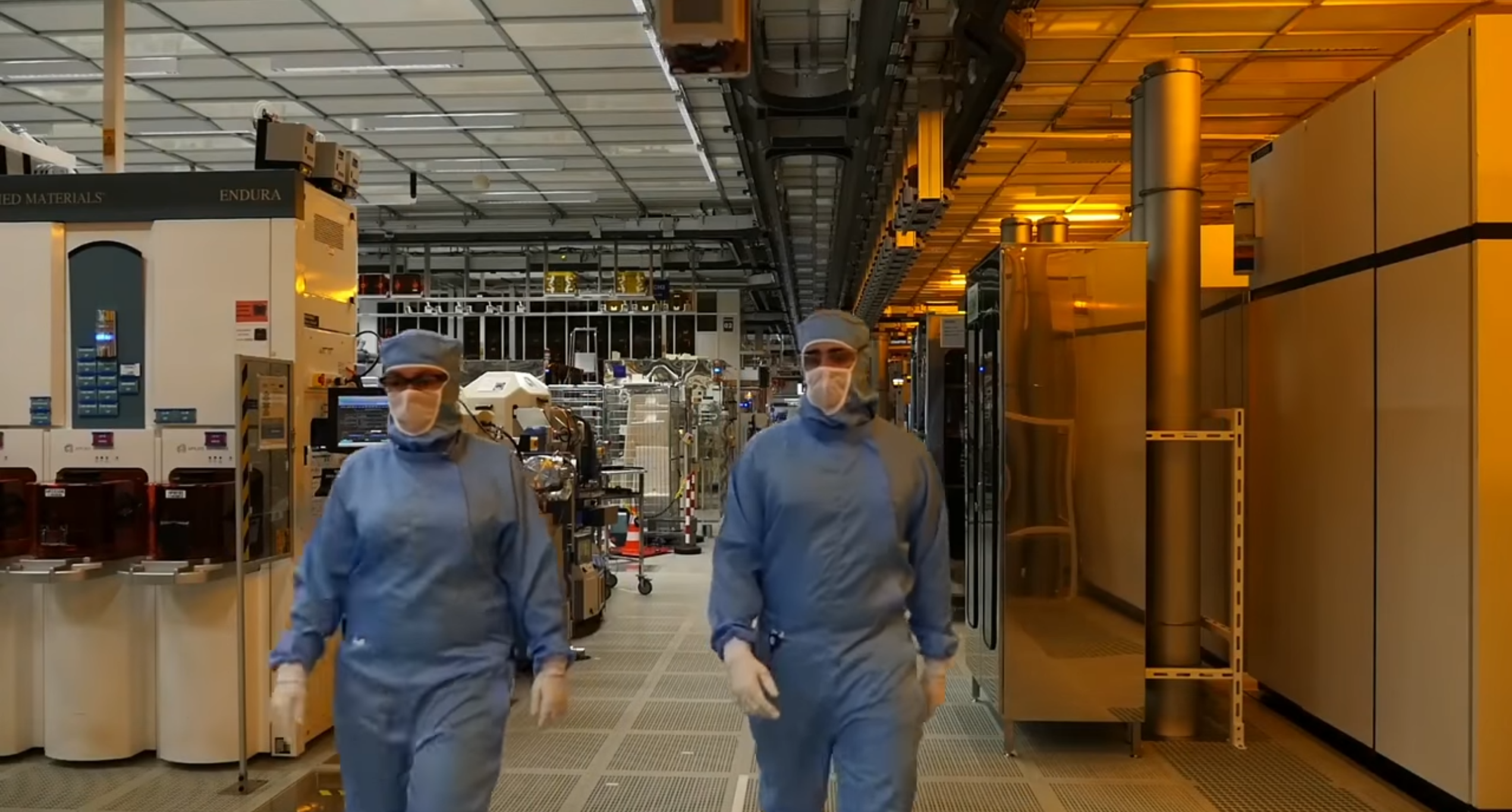
Image: Illustrative semiconductor cleanroom at STMicroelectronics, not a Samsung facility. STMicroelectronics / Una tantum. Image source. CC BY 3.0.