How UCIe 4.0 makes room for memory at the die edge
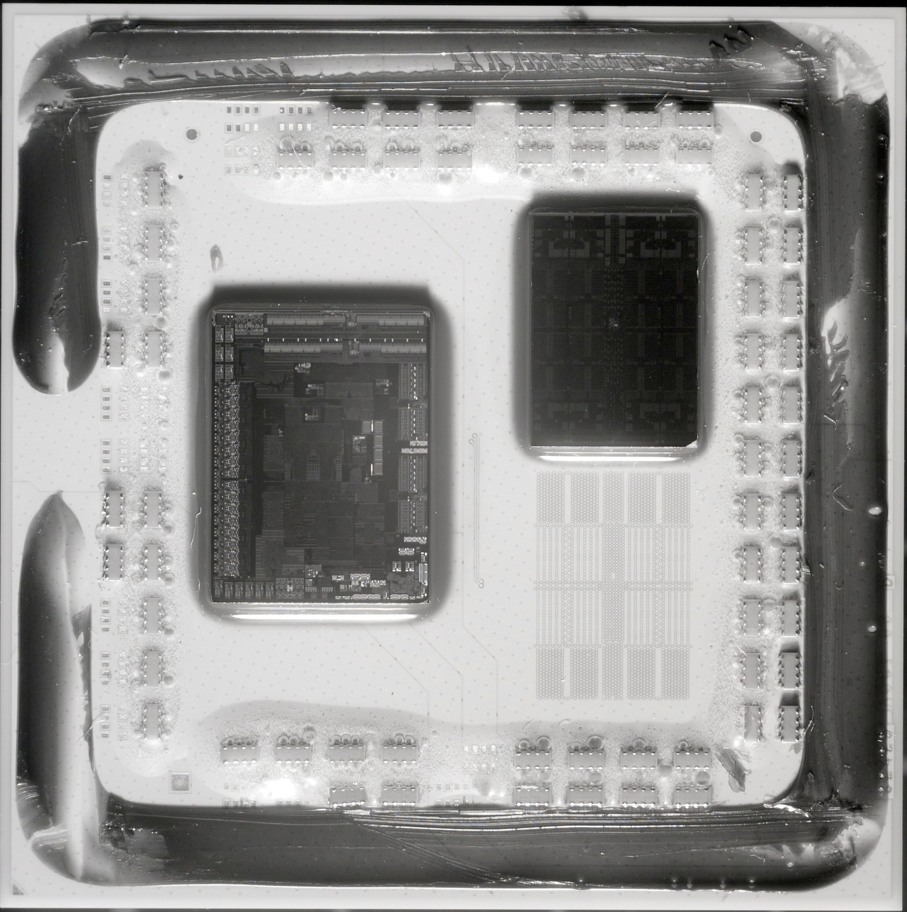
Image: Fritzchens Fritz · CC0 1.0
UCIe 4.0 gives a system-on-chip a standard way to talk to a memory logic die in the same package. The new UCIe.mem protocol runs over the existing UCIe physical layer and adapter, so designers can build on that interface without specifying the same memory technology behind every logic die. That leaves the package designer with a choice about what sits beyond the link as well as how much of the compute die to devote to reaching it.
Memory links compete for space with accelerator and I/O connections along the edge of a compute die. Increasing the lane count uses more interface circuitry, bumps and routing, which can squeeze another connection even when the package still has room elsewhere. If the protocol carries more payload in each transfer, the same bandwidth target can require less raw traffic. Whether that saves a lane or leaves spare bandwidth on a link of the same width depends on the configurations available to the design.
How much bandwidth fits along the die edge
The UCIe Consortium quotes data efficiency of up to 93.75% for UCIe.mem and a die edge bandwidth density of about 2.5 TB/s per millimetre. The efficiency figure is about how much of the link’s data traffic carries payload; the density figure relates bandwidth to the length of silicon edge occupied. Neither says how fast a workload can read from memory. By the time a request reaches the logic die, its controller and memory devices have to serve it. The size of those requests and how many the controller can handle at once determine how much of the available bandwidth an application sees.
For UCIe-S at 48 and 64 GT/s, the revision also offers a new bump map that the consortium says increases bandwidth per millimetre of die edge by about 20% and bandwidth per unit of interface area by about 10%. Those figures can pull a design in different directions. A compute die that already has enough memory bandwidth might recover edge for another interface, while a design with a fixed footprint might use the same change to move more data. In either case the package still has to accommodate the routes from the revised bump pattern.
There is a different constraint when the package has room for the link but runs up against its power budget. For an optional profile at 64 GT/s, the consortium reports an energy efficiency improvement of 30% to 80%. The range describes the link profile. It cannot be applied to the whole package, where memory, compute and the other links still draw power of their own.
Bringing separately designed dies into one package
An SoC and a memory logic die can share a protocol and still need work to operate as a pair. Both ends have to support compatible profiles and the package interconnect has to meet the electrical requirements at the intended speed. Once the connection is running, the slower part of the path sets the sustained throughput: more link bandwidth gives little back if the memory controller is already fully occupied, while faster memory can sit waiting behind a congested link to the SoC.
UCIe 4.0 also adds protected management communications, more control over resets and optional reporting on link health. If a package combines dies from several suppliers, those features help the system identify a chiplet and respond to faults on its link. They complement the common interface without establishing that a particular pairing has passed qualification. ASRA and imec’s separate automotive requirements address interoperability in vehicle SoCs, where safety and operating life impose constraints of their own.
Sources: UCIe Consortium release and technical figures; UCIe 4.0 specification request; ASRA and imec automotive announcement.