Photon Bridge spreads the optical load across more lasers
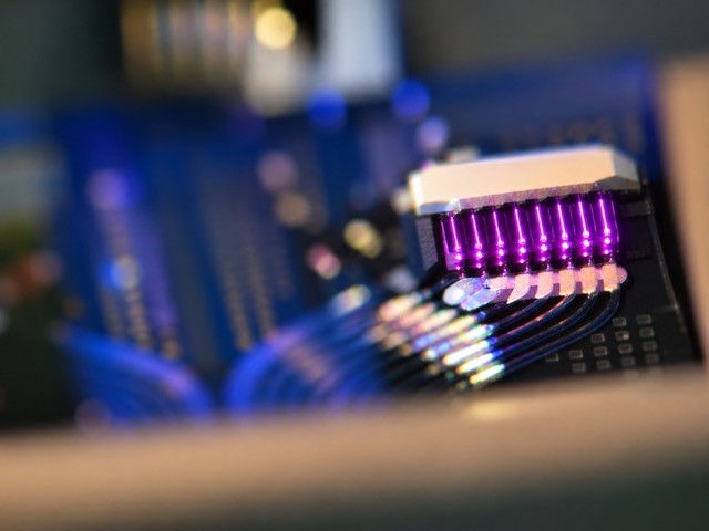
Photon Bridge has raised €10m to develop laser sources for optical interconnects in AI systems. Its architecture combines light from multiple semiconductor lasers and places the wavelength multiplexer on the silicon interposer alongside them. The aim is to make the required optical output achievable with lasers operating at moderate power. As chief executive Paul Marchal puts it, “we move that scaling challenge into the architecture”.
The company is working with distributed feedback lasers, with a proposed path to eight, 16 and 32 wavelengths. Each wavelength has to reach the optical engine with enough power left after coupling and propagation losses. Dividing the work across an array reduces the output demanded from an individual die, which Photon Bridge argues should improve yield and allow it to work with more InP foundries.
The integration step brings light from III-V laser dies into silicon waveguides while making their electrical connections. Its cantilever structures are designed to align the optical interfaces during flip-chip attachment, combining two operations in the same assembly step. Photon Bridge says placement accuracy of about 2 µm becomes effective optical alignment better than 200 nm, without active alignment.
A process that achieves that alignment passively would avoid a separate optical adjustment after placement. Its value in manufacturing depends on achieving the result repeatedly across attachments. The optical interface has to retain the required coupling after the electrical bonds have formed and as the completed assembly changes temperature.
Testing the die before the attachment
Photon Bridge describes a flow using tested, III-V dies that have passed burn-in testing with a flip-chip process intended to fit outsourced semiconductor assembly and test operations. Screening the laser before attachment avoids spending further assembly work on a die already known to fail. The attachment still adds its own yield term: a good laser can lose usable output through a poor optical connection.
The silicon platform uses 2 µm waveguides, appreciably thicker than the 220 nm platform the company uses for its comparison. Photon Bridge attributes greater handling of optical power and reduced sensitivity to manufacturing variation to that geometry. Its proposed multiplexer and laser array are built around those characteristics.
Amadeus APEX Technology Fund and 360 Capital jointly led the financing round. The money supports product development and customer qualification, with first samples planned for 2027 and preparation for volume manufacturing from 2028. Photon Bridge also plans to expand its Eindhoven team.